Mar 4 2011
In an effort to make it easier to build inexpensive, next-generation silicon-based electro-optical chips, which allow computers to move information with light and electricity, a University of Washington photonics professor, Dr. Michael Hochberg and his research team are developing design tools and using commercial nanofabrication tools.
Silicon optical chips are critical to the Air Force because of their size, weight, power, rapid cycle time, program risk reduction and the improvements they can offer in data communications, lasers and detectors.
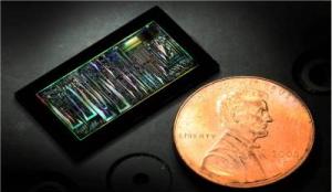
 This is a dark-field optical image of a silicon photonic chip is shown in comparison to the size of a penny.
The Air Force Office of Scientific Research is funding this effort in silicon photonics called "Optoelectronic Systems Integration in Silicon" at UW's Nanophotonics Lab in Seattle. OpSIS is hosted by UW's Institute for Photonic Integration. Hochberg is in charge of the OpSIS research program, the Nanophotonics Lab and the Institute for Photonic Integration.
Hochberg emphasizes that the funding from the Air Force Research Laboratory and AFOSR is a critical component in getting the effort off the ground because it provides both a strong technical validation, and the resources to get started on the project.
Unlike most research groups that are designing, building and testing silicon photonic devices or optical chips in-house rather than by using commercial chip fabrication facilities, the UW researchers are using shared infrastructure at the foundry at BAE Systems in Manassas, Virginia. There they are working toward creating high-end, on-shore manufacturing capabilities that will be ultimately made available to the wider community. In the past few years, complex photonic circuitry has not been accessible to researchers because of the expense and a lack of standard processes.
The UW researchers are working on system design and validation so they can imitate what's been done in electronics by stabilizing and characterizing some processes so that the transition from photonics to systems can be smooth.
"The OpSIS program will help advance the field of silicon photonics by bringing prototyping capability within reach of startup companies and researchers," said Hochberg. "They will provide design rules, device design support and design-flow development so that even non-experts will be able to design and integrate photonics and electronics."
Silicon photonics has developed over the last decade, and the transition from using devices to systems is something that has only recently occurred.
"The digital electronics revolution over the past 40 years has had a transformative effect on how the Air Force systems are built, and we're hoping to have a similar impact on photonic systems," he said.
The researchers' current goal is to work first on test runs for the new optical chips for commercial uses and on developing some software tools that will make the design process easier.
AFOSR program manager, Dr. Gernot S. Pomrenke, agrees with Prof. Hochberg. "Integrating silicon photonics will impact Air Force, DoD and commercial avionics," he said. "AFRL has been a leader in developing and supporting this technology over the last two decades and the OpSIS program will help in transitioning silicon photonics into new system capabilities."
Source: http://www.wpafb.af.mil/AFRL/afosr/