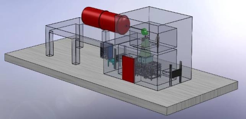
Silicon Genesis (SiGen) has completed the specifications of the new GenII PolyMax system, the company’s second-generation production system for manufacturing thin-silicon solar wafers.
 GenII Proton Implanter Design (Graphic: Business Wire)
SiGen had spent more than six years in development, testing of prototypes and evaluation of solar cell materials and collaborated with several solar cell and equipment partners for designing the GenII PolyMax system.
The PolyMax high volume manufacturing system provides waste-free wafering solution at lower cost and is an ideal substitute for wire saw processes being used in the industry. The system can fabricate thinner wafers than is producible with wire saw technology, enabling the industry to manufacture high-conversion-efficiency solar cells at lower cost.
SiGen’s beam-induced wafering technology will not only be used in the solar industry but can also produce high-quality thin materials for other emerging industry needs in packaging/3D structures and HB-LEDs using Sapphire, GaN, SiC, Germanium, GaAs and Silicon. The major advantage of this system is its ability to produce high-performance materials at reduced cost and at the same time maintains efficacy in complex end applications.
According to SiGen’s President and Chief Executive Officer, Francois Henley, the company believes that the severe pricing pressure of the solar industry drives the growth of the proton beam-induced wafering technology. The company unveiled its first beam-induced cleaving technology with 50 µm thick wafers utilizing a prototype 2 million volt high-energy proton implanter during the 2008 PVSEC Conference. The company’s partners and independent third party laboratories have tested and characterized these thin and ultrathin solar wafers.