A research team led by Miquel Salmeron from the Lawrence Berkeley National Laboratory (Berkeley Lab) of the U.S. Department of Energy (DOE) has detected the transportation pathways of an electrical charge from one molecule to another molecule in an organic thin film, paving the way to develop advanced organic or polymer electronic devices.
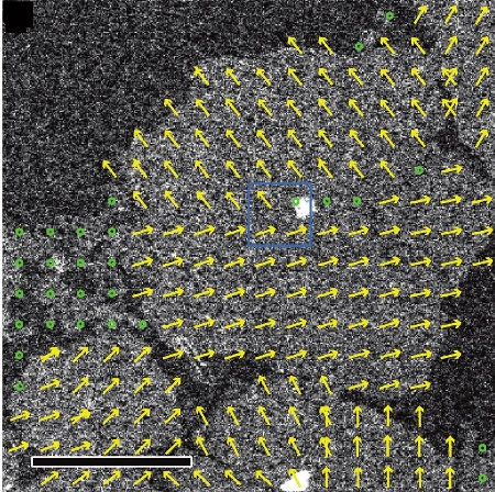
 Scanning transmission electron microscopy image of an organic thin film deposited on a silicon nitride membrane. Yellow arrows indicate the lattice orientation of each crystalline domain. Green circles mark polycrystalline areas. (Image from Berkeley Lab’s Molecular Foundry)
The researchers have also demonstrated the way to enhance conductivity of organic thin films by chemically modifying them. The experiment has been conducted at Berkeley Lab’s Molecular Foundry, a nanoscience center of DOE.
Salmeron commented that the research team was able to improve the conductivity of organic thin films by arranging their molecules in specific directions. Since chemists are already familiar with the method of fabricating organic thin films with that specific alignment, they can also use Berkeley Lab’s method to detect the molecular alignment and its impact on charge transportation between the molecules, thus opening the possibility to enhance the performance of yet-to-be-developed organic electronic devices.
In this experiment, the research team mapped the molecular film’s crystal structures using electron diffraction patterns. These molecular films were made of monolayers of shorter versions of polymers comprising lengthy chains of thiophene units. To map the monolayer molecular film’s crystal structure, the research team developed a unique strategy and used a transmission electron microscope at the Imaging and Manipulation of Nanostructures Facility of the Molecular Foundry. Structural crystallographic maps were generated by a computer analysis of the electron diffraction patterns that were obtained by scanning a parallel electron beam over the film.
Virginia Altoe, one of the researchers, informed that these maps provide uncompromised data of the degree of crystallinity, the structure and orientation of the domains, the orientation, symmetry and size of the unit cell, and any differences on the micro-scale, which are vital to know the electrical transport properties and structure of the organic thin films. The research team informed that it gained the structural information at the expense of some resolution and the structural mapping method can be employed for materials that have electron-based conductance. This method shows potential in a broad array of material research applications.