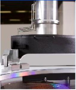
Applied Materials has introduced its latest dielectric etch system labeled the Applied Centura Avatar etch system that is designed to meet the challenges associated with the design of high density, terabit storage capacity, three-dimensional memory architecture.

The Centura Avatar etch system
Dr. Prabu Raja, Vice President and General Manger of the Etch Business at Applied, stated that the company leveraged its expertise in plasma technology to facilitate deep etching through multiple layer complex material stacks typical of 3D memory structures. The company has already dispatched more than 30 chambers to various customers.
Three-dimensional NAND memory arrays are flash devices with extremely high bit density and can accommodate as many as 64 memory cell layers. Designed and built from scratch, the Centura Avatar system is capable of etching trenches through multiple film layers of depth to width aspect ratio, 80:1. In order to perceive this proportion, one can compare it to the Washington monument that has an aspect ratio of 10:1. The system is also capable of etching structures with different depths at the same time. This feature facilitates the connection of memory cells to outer circuits by enabling the fabrication of staircase-like contact structures.
Applied Materials is set to exhibit the Avatar system along with other novel chip-making technologies at the SEMICON West 2012 from July 10 to 12.
Disclaimer: The views expressed here are those of the author expressed in their private capacity and do not necessarily represent the views of AZoM.com Limited T/A AZoNetwork the owner and operator of this website. This disclaimer forms part of the Terms and conditions of use of this website.