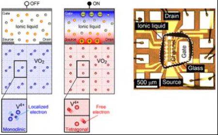
A research team at the RIKEN Advanced Science Institute has created a first-of-its-kind transistor that utilizes the electrostatic build-up of electrical charge on a strongly-correlated material’s surface to activate bulk transformation of electronic state.
 A schematic and an optical micrograph of a new transistor based on VO2 enabling electrical switching of the state of matter (credit: RIKEN)
Activated by an electric potential of only 1 V and operational at room temperature, the switching mechanism offers a unique building block to develop optical switches, non-volatile memory, and low power devices on the basis of a new device concept. The research team has reported their breakthrough device in the journal, Nature.
The transistor utilizes an electric-double layer to alter the charge density on the surface of vanadium dioxide, a proven conventional strongly-correlated material. The powerful electron-lattice coupling and electron correlation in vanadium dioxide enable this surface charge to delocalize the localized electrons in the bulk, thus significantly magnifying the electronic phase change. With an electric potential of only 1 V, the research team has demonstrated the transformation of the material from an insulator to a conductor and activation of a remarkable 1,000-time drop in resistance.
However, utilizing synchrotron radiation from RIKEN's SPring-8 facility in Harima, the research team has demonstrated that not only the electronic phase but also the crystal structure of the vanadium dioxide changes during this insulator-to-metal transition. The structure has changed from monoclinic to tetragonal. Electric-field activated bulk transition of this type is not possible with traditional semiconductor-based electronics and shows promise in a variety of applications.
The novel switching mechanism advances the transistors to a new level, illustrating that a tiny electric potential is adequate to manipulate macroscopic electronic states and paving the way to harnessing the state of matter.