Scientists at A*STAR’s Institute of Materials Research and Engineering (IMRE) have devised a ground-breaking technique that utilizes metal-laced nano-scale structures to create sharp, full-spectrum color images at 100,000 dpi, without using dyes or inks.

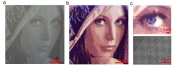
A colored nanoscale rendition of a standard test image used in image processing experiments - (a) Before the addition of metal in the nanostructures, the image has only grayscale tones as observed under an optical microscope. (b) Colors are observed using the same optical microscope after addition of the metal layers to the nanostrucutres and in specific patterns. (c) Zooming into the image with the same setup, the specular reflection at the corner of the eye is observed showing the refined colour detail that the new method is able to achieve. The region indicated (bottom right) is made up of nanostructures as observed in the electron micrograph.
Existing industrial printers like laserjet and inkjet printers are capable of creating images at only 10,000 dpi and research grade techniques can dispense dyes for only one-color images. This innovative technique enables coloring to be processed as a lithographic matter instead of an inking matter, thus paving the way to transform the method of printing images and develop applications for use in high density optical data storage and high-resolution reflective color displays.
Stained glass, which is made by adding small metal fragments into the glass, was the inspiration for this technique. It was discovered that stained glass gets its colors through the scattering of light by nanoparticles present in these metal fragments. Utilizing a similar concept and cutting-edge nanotechnology tools, the IMRE researchers accurately patterned metal nanostructures on a surface in order to scatter the light to get the color images.
Dr Karthik Kumar, one of the researchers, stated that the printed color image’s resolution relies on the spacing and size of individual ‘nanodots’ of color. The image’s resolution is higher when the size is smaller and the dots are closer. With the capability to precisely position these ultra-small color dots, the researchers demonstrated the peak theoretical print color resolution of 100,000 dpi.
Project leader, Dr Joel Yang stated that rather than utilizing different dyes for various colors, the researchers encoded color data into the position and size of small metal disks, which then interplayed with light through plasmon resonances. The researchers developed a database of colors corresponding to a particular pattern, spacing and size of nanostructures, which were then placed accordingly. The ‘numbers’ were defined by the positions and sizes of these nanostructures. However, rather than sequentially coloring every space with a different ink, the researchers deposited an ultrathin uniform metal film throughout the whole image, resulting in the appearance of the ‘encoded’ colors instantaneously.
The IMRE had also partnered with A*STAR’s Institute of High Performance Computing (IHPC) for the pattern design utilizing computer simulation and modeling. At present, the researchers together with A*STAR’s technology transfer arm, Exploit Technologies, are working on finding potential partners and also exploring ways to license the technology.
The work was reported in Nature Nanotechnology.
Disclaimer: The views expressed here are those of the author expressed in their private capacity and do not necessarily represent the views of AZoM.com Limited T/A AZoNetwork the owner and operator of this website. This disclaimer forms part of the Terms and conditions of use of this website.