More material could be saved when manufacturing wafers in future. Ultra-thin saws made of carbon nanotubes and diamond would be able to cut through silicon wafers with minimum kerf loss. A new method makes it possible to manufacture the saw wires.
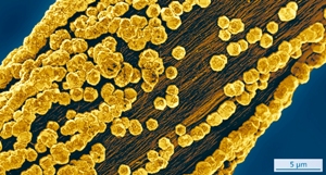
 New ultra-thin saw wire for cutting silicon wafers: diamond on top of carbon nanotubes. © Fraunhofer IWM
You can’t saw without producing sawdust – and that can be expensive if, for example, the “dust” comes from wafer manufacturing in the photovoltaic and semiconductor industries, where relatively high kerf loss has been accepted as an unavoidable, if highly regrettable, fact of life. But now scientists from the Fraunhofer Institute for Mechanics of Materials IWM in Freiburg together with colleagues from the Australian Commonwealth Scientific and Industrial Research Organisation CSIRO have developed a saw wire that is set to effect dramatic reductions in kerf loss: in place of diamond-impregnated steel wires, the researchers use ultra-thin and extremely stable threads made of carbon nanotubes coated with diamond.
The potential of coated carbon nanotubes has long been understood: possible applications include its use as a hard and tough composite material or as a component of highly sensitive sensors and thermoelectric generators. However, the new material is extremely difficult to synthesize. Diamonds only grow under extreme conditions – at temperatures of around 900 degrees Celsius in an atmosphere containing hydrocarbons. Growing diamonds on nanotubes is a tricky proposition, because carbon tends to form graphite. In order to catalyse the formation of the diamond phase, it’s necessary to use reactive hydrogen to prohibit the deposition of graphite. However, this process also damages the carbon nanotubes.
But the IWM scientist Manuel Mee found a solution for protecting the fine carbon nanotubes, which grow like forests on a substrate: “During our first experiments, fused silica from the reaction chamber accidentally came into contact with the coating plasma. It settled on the substrate and protected it against the aggressive hydrogen.” And to his surprise, diamonds actually grew on this layer. “What followed was careful, painstaking work,” points out Mee. “We had to study the silicon oxide layer, which was deposited in an undefined manner, and find a method of controlling the deposition and optimizing the process.” Tests with a transmission electron microscope at CSIRO’s lab in Australia revealed that the nanotubes actually survived under their protective layer.
A German-Australian success story
How exactly to proceed from there was the question that now faced the scientists. If they found a way to coat with diamond the nanothreads that the CSIRO specialists make from nanotubes, these diamond-coated nanothreads could be used to manufacture ultra-thin saws capable of cutting through silicon wafers for instance. The Australian team at CSIRO is one of the principal global experts with the know-how to manufacture yarns from carbon nanotubes. The manufacturing process requires special carbon nanotube “forests”, which can be extracted as an ultra-thin “felt” and twisted into a very thin yarn ten to twenty micrometers in diameter. In principle, this diamond-coated yarn is the ideal material on which to base a new generation of saws, which could be used in the solar industry for example. As Mee explains: “The new saw wires held out the promise of being far superior to traditional steel wires. Because of their high tensile strength, they can be manufactured much thinner than steel wires – and that means significantly less kerf loss.”
In the meantime, the physicist has managed to implement his idea. A joint patent application by Fraunhofer and CSIRO has already been filed for the method and corresponding products. Mee and his colleagues are currently carrying out sawing tests. “To be able to show our partners in industry the potential the technology holds,” says Mee, “we have to demonstrate how it can help solar companies to save material when processing wafers.”