Sep 17 2013
A team of researchers led by San Francisco State University’s Weining Man is the first to build and demonstrate the ability of two-dimensional disordered photonic band gap material, designed to be a platform to control light in unprecedented ways.
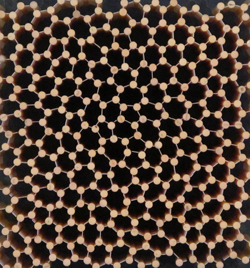
 Man and her colleagues designed and built a hyperuniform disordered photonic bandgap structure, seen above, using aluminum rods and a wall network, allowing them to demonstrate the ability of such material to steer light in unprecedented ways.
The new material could allow researchers to manipulate the flow and radiation of light in new ways by breaking away from the highly angular and constrained pathways for light dictated inside orderly photonic crystals. Instead, the material could lead to arbitrarily shaped, wavy, curved, and sharply bending ways to steer light, Man and her colleagues say.
The findings were published in the Sept. 16 issue of the Proceedings of the National Academy of Sciences.
Although the applications are far in the future, the new materials may be used for more efficient solar panels and illuminated displays. The “free-form” light guides within the materials could be especially useful in designing compact optical circuits for signal processing and telecommunications.
Photonic band gap materials help to steer photons -- light -- in the same way that semiconductors steer the flow of electrons in modern electronics. They accomplish this by blocking “light of a certain energy, or frequency, so that it won’t be able to propagate or exist in the material,” said Man, an assistant professor of physics and astronomy.
Photonic band gap materials are rare in nature, although they can be seen on the iridescent wings of some butterflies or on opals, where certain wavelengths of light are blocked from entering at all angles.
It had been a longstanding belief that a photonic band gap within constructed materials must rely on the reflection in layers of crystalline structures such as silicon crystals, Man said. But more recently, her collaborators at the University of Surrey, Princeton University and New York University have predicted using numerical simulations that it is possible to have photonic band gap in disordered structures.
An orderly periodic pattern, such as the tiles on a bathroom floor, can only be constructed with certain shapes like hexagons or triangles or squares. For this reason, periodic, orderly photonic band gap materials are limited to conveying light only in special pathways along particular crystalline directions.
The material made by Man and her colleagues is disorderly, and therefore not limited to particular rotational symmetry like bathroom tiles. That means they can be built to be isotropic, or look the same in all directions. This combination of features, she said, “provides a free-form platform so that we can choose any kind of bending or curved passes to direct the light’s flow.”
Since the material is identical in all directions, it has the same photonic properties in all directions. This quality might prove useful in future applications that need to collect or radiate light in a uniform way, such as a solar energy panel or a display.
“Scientifically, it’s terrific to prove that a disordered structure can have a photonic band gap, for all polarizations in all directions,” Man added.
The researchers started with a “point pattern” to design the disordered materials. The design was then converted into a computer file for three-dimensional printing of the base structure, with precise holes and slots that guided the assembly of alumina rods and sheets. Peter Verdone, a staff member in the Department of Physics and Astronomy, contributed to the three-dimensional printing files. The modular design -- slightly like Lego brand bricks -- allowed individual pieces to be removed or added to create new arbitrary shapes of waveguides.
Five SF State students and Man performed all the experimental work in this project, co-authoring the PNAS paper with Man’s collaborators. The material is built on a centimeter-scale -- large enough to be held in the hand -- and was tested with microwaves, which have a longer wavelength than visible light.
After the successful demonstration with microwaves, Man said it is straightforward to scale down the material to channel the shorter wavelengths of visible and infrared light. Two of Man’s graduate students, Sam Tsitrin and Geev Nahal, are working on the design and fabrication of these materials at the scale of 500 nanometers with the support of a National Science Foundation grant.