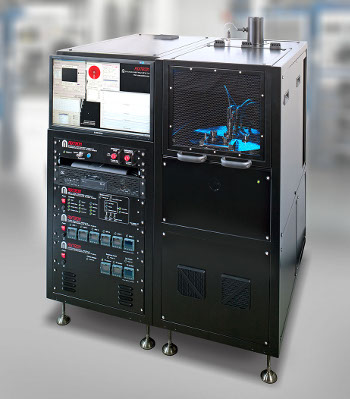
AIXTRON SE today announced a new purchase order from the University of Massachusetts (UMass) Lowell, USA, for a BM deposition system equipped for processing 4-inch substrates. The equipment has been shipped to the university’s recently completed Emerging Technologies and Innovation Center (ETIC), which is a state-of-the-art shared research facility for academics, start-ups and companies-inresidence.
Thomas Ferraguto, Director of Nanofabrication Cleanroom Operations at Massachusetts’ Core Research Facility, comments:
“We will use the new system for the integration of carbon nanotubes (CNT) and graphene into a large variety of electronic applications ranging from high frequency transistors, energy storage and flexible electronics. The engineering community here is eager to exploit graphene and carbon nanotube properties. The BM system provides a flexible, reliable platform for depositing these materials.”

Furthermore, from a shared-facility point of view, the BM system is advantageous as it enables multiple users with consumables tracking; this ensures proper assignment of operating costs to the appropriate research or commercial end user.
Accessing the unique properties of graphene and carbon nanotubes for commercial applications is the key challenge for future R&D and manufacturing. AIXTRON offers a highly flexible system which can deposit both graphene and CNT materials with precisely controlled critical surface dimensions, enabling manufacturers to improve throughput, performance, yield and quality.
The BM system also features automatic process control, easy recipe editing, an integrated process camera and remote operation via TCP/IP networking. Researchers worldwide use the systems to explore new possibilities and to provide services to others in the scientific, engineering and industrial communities.
About AIXTRON
AIXTRON is a leading provider of deposition equipment to the semiconductor industry. The Company's technology solutions are used by a diverse range of customers worldwide to build advanced components for electronic and opto-electronic applications based on compound, silicon, or organic semiconductor materials and more recently carbon nanostructures.
Such components are used in display technology, signal and lighting technology, fiber communication networks, wireless and cell telephony applications, optical and electronic data storage, computer technology as well as a wide range of other high-tech applications.