Oct 31 2013
How’s this for precision? Researchers with the University of Houston Cullen College of Engineering are developing technology to knock single atoms off a silicon wafer without disturbing atoms of other materials nearby.
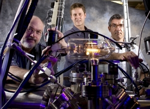
 Chemical and biomolecular engineering faculty members Vince Donnelly (left) and Demetre Economou (right) won a $150,000 grant from the National Science Foundation to develop a technique to etch materials with atomic layer precision. They are shown here with ECE Associate Professor Paul Ruchhoeft (center)
Chemical and biomolecular engineering professor Vince Donnelly and Demetre Economou, Hugh Roy and Lilly Cranz Cullen Distinguished University Chair with that same department, are supported in this project by an 18-month, $150,000 grant from the National Science Foundation.
Their effort focuses on plasma etching, where ions are shot at a material to create extremely small patterns and features. Specifically, they are exploring ways to etch wafers of silicon with atomic precision. Such an advance could be used to create radically smaller and more powerful integrated circuits, which are at the heart of practically all computing and electronic devices.
To create these extremely fine and precise features, researchers use a mask – essentially a stencil –that has the desired patterns already formed on it. The masked substrate is then placed in a plasma. There, some of the plasma’s ions pass through the mask’s patterned holes and etch away the layer just beneath it, creating a perfect copy.
The big challenge to this approach, though, is controlling the kinetic energy – the energy of movement – of the ions that pass through the mask.
As the ions strike the silicon wafer, the wafer becomes electrically charged. This charge ends up slightly repelling the positively charged ions – essentially lowering their kinetic energy. As a result, the beam becomes too weak to etch away the underlying material. The industry overcomes this problem by using AC voltage to neutralize charge. This however, leads to a loss of ion energy control.
“The goal is to have all the ions coming in with the same energy so you can selectively etch one material and not etch another,” said Donnelly. “The materials have a threshold for etching. You have to exceed a certain energy to etch a material. If you can select the energy of the ions to be between the thresholds of silicon and silicon dioxide, for example, you can etch silicon and absolutely not the silicon dioxide.”
Donnelly and Economou, though, believe they can overcome this problem by applying small, quick bursts of positive voltage to the silicon wafer. Doing so, they said, should neutralize the wafer’s charge. As a result, the ion beam can be set to and remain at a kinetic energy that is in the sweet spot between two materials such as silicon and silicon dioxide etching.
“Atomic-scale etching should contribute to the creation of the most advanced integrated circuits ever built. If we can control the kinetic energy of the ions, we can pattern the silicon wafer with that high level of precision,” said Donnelly.