Mar 29 2014
Tufts University engineers have demonstrated that it is possible to generate nanostructures from silk in an environmentally friendly process that uses water as a developing agent and standard fabrication techniques.
This approach provides a green alternative to the toxic materials commonly used in nanofabrication while delivering fabrication quality comparable to conventional synthetic polymers. Nanofabrication is at the heart of manufacture of semi-conductors and other electronic and photonic devices.
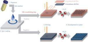
 At Tufts University School of Engineering, optical-grade silk fibroin aqueous solution, obtained from the cocoons of the Bombyx mori caterpillar, was placed on a substrate and spin-coated to form a silk film. Both positive and negative resists were formed and developed using water. Credit: Tufts University
The paper describing this work, "All Water-based Electron Beam Lithography Using Silk as a Positive, Negative and Biofunctional Resist," appears in Nature Nanotechnology, published online March 23 in advance of print publication.
"In a world that strives to reduce toxic footprints associated with manufacturing, our laboratory is exploring biopolymers, and silk in particular, as a candidate material to replace plastics in many high-technology applications," said Frank C. Doble Professor of Biomedical Engineering Fiorenzo Omenetto, Ph.D., senior researcher on the work.
Nanofabrication involves high-resolution patterning with features so small that they have at least one dimension no larger than 100 nanometers (nm)—the size of particles filtered out by surgical masks. Nanoscale fabrication is usually obtained depositing thin films of customized polymers, called "resists," onto silicon wafers. Each resist layer is successively patterned by using light or electrons (via electron beam lithography) to expose the part of the resist not covered by a mask. Subsequently, positive resists are dissolved when subjected to a developer while negative resists remain behind after development. The composition and configuration of the layers determine the properties of the structure.
Developing a resist typically requires toxic chemicals, which need careful, and costly, handling and disposal. Significant advances have been made using "green" resists that can be developed with water, but these techniques have lacked the desired precision and scalability.
"In contrast, our process is entirely water-based, starting with the silk aqueous solution and ending with simple development of the exposed silk film in water, and the resolution achieved was comparable to one of the commonly used synthetic polymers," said Omenetto, who holds a professorship in the Department of Physics at Tufts School of Arts and Sciences in addition to his appointment in the School of Engineering. "A variety of manufacturing industries, high-tech companies and academic labs could ultimately benefit from clean rooms that are also green."
For this work, the Tufts engineers fabricated nanoscale photonic lattices using both neat silk and functionalized silk doped with quantum dots, green fluorescent proteins (GFPs) or horseradish peroxidase (HRP).
"By showing that biomolecules of the enzyme HRP remained active after the electron beam nanofabrication process, we demonstrated the feasibility of fabricating biologically active silk sensing devices, something not currently available," said Benedetto Marelli, Ph.D. Marelli is a post-doctoral associate in Omenetto's laboratory and a lead co-author on the paper with former Omenetto post doctoral associate Sunghwan Kim, Ph.D., now a professor in Ajou, Korea.
This research builds on previous work by Omenetto and his collaborators at the Tufts School of Engineering. In the past, they had shown that silk could be nanofabricated, but those processes required starting with other nanosized materials. This is the first time that silk has been fabricated to begin the nanofabrication manufacturing chain.