Jun 11 2014
Ferroelectric materials like barium titanate, a ceramic used in capacitors, are essential to many electronic devices. Typical ferroelectric materials develop features called domain walls with unusual properties – such as lines of electrical conduction completely different from the surrounding material. These properties are technologically useful but poorly understood.
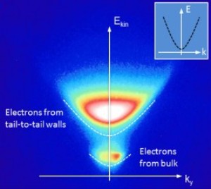
 The kinetic energy distribution of emitted photoelectrons when a sample is illuminated with X-rays at 641.2 eV. Electrons emitted at domain walls with enhanced electronic conduction in ErMnO3 travel with more kinetic energy, giving the walls a distinct appearance in X-PEEM images. Credit: Applied Physics Letters/ Jakob Schaab, et. al.
Now an international team of scientists has demonstrated the ability of a powerful imaging tool to provide new insight into the mystery of why domain walls behave in their peculiar ways. They report their results in the journal Applied Physics Letters, from AIP Publishing – work that promises to analyze so far unexplored domain wall properties that may lead to improved solar panels, electronic sensors, computer memory, and other applications.
Ferroelectric domain walls separate regions of material with different electric polarization orientations, and their physical properties can be completely different from the surrounding bulk material. Over the years, scientists have tried many different approaches to understand domain walls’ funky properties.
A technique called scanning probe microscopy has provided valuable insight into domain wall nanophysics by measuring a material’s electrical or mechanical response to a tiny, sharp-tipped probe. The scanning approach, however, is rather slow when high-resolution images are required, and may also produce unwanted measurement side effects due, for example, to contact resistance or inhomogeneous probe fields.
An alternative imaging method called X-ray photoemission electron microscopy (X-PEEM) allows researchers to bypass many of these limitations, but until now no one knew if it could capture the details of skinny domain walls, which can be only a few atoms thick. An international team of researchers from four different countries decided to join forces to test X-PEEM on domain walls in a model ferroelectric material called erbium manganese oxide (ErMnO3).
“X-PEEM is a particularly interesting tool because it allows for studying properties such as the chemistry, electronic structure, and symmetry of a material,” said Dennis Meier, a junior research team leader at the Swiss Federal Institute of Technology in Zurich and corresponding author on the new paper. Together with Ingo Krug, an instrument and beamline scientist at Technische Universität Berlin, he devised the X-PEEM experiments on domain walls using a state-of-the-art microscope (SPECS FE-LEEM P90 AC) at the synchrotron BESSY II in Berlin, Germany. X-PEEM works by bombarding a sample with X-rays that excite electrons in the material, and then uses variations in the electron emission to create image contrast.
Meier and his colleagues found that X-PEEM could image electrically conducting domain walls extremely well. In ErMnO3 these walls are so-called tail-to-tail domain walls separating regions with polarizations that point away from each other.
“In general, it is very difficult to directly image ferroelectric domain walls,” Meier said. “In our X-PEEM data, however, the tail-to-tail domain walls can easily be identified and are clearly separate from the surrounding bulk. We did not expect this remarkable sensitivity.”
The tail-to-tail walls appear so vividly in the X-PEEM images because their enhanced electronic conduction properties help them to better compensate for charging effects than the rest of the material when illuminated with X-rays. The difference causes electrons emitted at tail-to-tail domain walls to travel with more kinetic energy, giving the domains walls a distinct appearance.
The researchers see their work as just the first step in a long journey toward a better understanding of domain wall nanophysics. One of the advantages of X-PEEM is that it can be used to study the behavior of specific elements in the vicinity of a domain wall, Meier said, adding that the team plans to conduct such experiments soon.
The unusual behavior of ferroelectric domain walls, together with the fact that the walls can be easily created, moved, and erased has triggered an enormous interest in the field, Meier said. By proving X-PEEM a feasible tool for imaging and analyzing ferroelectric domain walls, the team hopes to open the door to important experiments that will speed the design of the next generation of electronic devices, he said.
The article, "Imaging and characterization of conducting ferroelectric domain walls by photoemission electron microscopy" is authored by Jakob Schaab, Ingo P. Krug, Florian Nickel, Daniel M. Gottlob, Hattice Doganay, Andres Cano, Mario Hentschel, Zewu Yan, E. Bourret-Courchesne, Claus M. Schneider, Ramamoorthy Ramesh, and Dennis Meier. It will be published in Applied Physics Letters on June 10, 2014 (DOI:10.1063/1.4879260). After that date, it may be accessed at: http://scitation.aip.org/content/aip/journal/apl/104/23/10.1063/1.4879260
ABOUT THE JOURNAL
Applied Physics Letters features concise, rapid reports on significant new findings in applied physics. The journal covers new experimental and theoretical research on applications of physics phenomena related to all branches of science, engineering, and modern technology. See: http://apl.aip.org