Mar 12 2015
Physicists from Forschungszentrum Jülich have developed a criterion with which scientists can seek suitable substrate materials for graphene in a targeted way. Interactions with the substrate material often lead to a loss of the amazing properties that characterize this special form of carbon. Together with partners at other institutions, the scientists were able to demonstrate that the influence exerted by the substrate on the electronic properties of graphene can be estimated by means of a simple structural parameter. The related publication was chosen as the Editor's Suggestion of the journal Physical Review Letters.
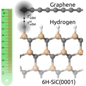
 Graphene on a silicon carbide substrate whose surface has been treated with hydrogen in order to electrically decouple the graphene. The distance between the two layers, minus the respective van der Waals radii, gives an approximate value for the interaction strength. Copyright: Sforzini et al., Physical Review Letters, Copyright 2015 by The American Physical Society
Harder than diamond, tougher than steel and many times more conductive than silicon—these and further extraordinary properties are the reason why graphene is intensively studied worldwide. The material is only one atomic layer thick. Its use, however, is so far mostly limited to laboratory experiments. One of the major tasks on the way to practical applications is the search for suitable substrate materials without which the extremely thin material is of little use.
“We simply wanted to find an accessible parameter which can be used to compare different substrates directly,” reports Dr. François Bocquet. “The decisive criterion turned out to be the atomic distance between the graphene layer and the underlying substrate,” explains the physicist and Helmholtz postdoc at Jülich's Peter Grünberg Institute (PGI-3).
Considering the van der Waals radius—a known value for the size of atoms in their free state—the strength of the interaction can be calculated directly from the distance. Computer simulations performed by scientists from the Berlin Fritz Haber Institute of the Max Planck Society confirm this result.
Highly precise measurements with X-rays
At the Diamond synchrotron radiation source in Didcot, Oxfordshire, UK,François Bocquet and his colleagues used X-rays to measure the distance between graphene and its substrate at a precision down to the picometre range. One picometre corresponds to one thousandth of a nanometre, i.e. one billionth of a millimetre. Length differences much smaller than the atomic diameter can thus be determined.
The scientists used silicon carbide with hydrogen applied to its surface as a sample. Scientists from the Max Planck Institute for Solid State Research in Stuttgart only developed the specially prepared semiconductor material a few years ago for use as a substrate material for graphene. In contrast to the usual metallic substrates, a graphene layer deposited on this material is practically interaction-free and thus retains its extraordinary electrical properties.
“With the emergence of this new class of substrates, it was time for a new criterion with which even very weak interactions can be detected precisely,” explains the director at the Jülich Peter Grünberg Institute, Prof. Stefan Tautz, who heads the subinstitute Functional Nanostructures at Surfaces (PGI-3). “With the techniques available so far, for example photoelectron spectroscopy, the degree of interaction with the substrate could only be deduced indirectly. Bonds as weak as these could hardly be detected.”