Apr 29 2015
As microchip feature dimensions approach atomic scale, it becomes formidably difficult to measure their size and shape. According to the International Technology Roadmap for Semiconductors, within the next couple of years the typical length of a transistor’s “gate” – its on-off switch – will be less than 20 nanometers (nm, billionths of a meter).
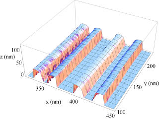
 A three-dimensional reconstruction of chip features from measurements using the NIST model-library method.
Meeting production tolerances for devices with those dimensions will require measurements with a minimum uncertainty around 0.3 nm. And the task is poised to get harder: By 2020, gate lengths are expected to shrink to around 12.5 nm, demanding uncertainties in the range of 0.2 nm – about the width of one silicon atom.
That places extraordinary pressure on chip makers to improve process control. In general, fabricators gauge the critical dimensions of a gate (or any feature) by detecting its edges, using an instrument called a scanning electron microscope (SEM). SEMs measure the number of low-energy electrons ejected from a sample when it is hit with a beam of high-energy electrons; those amounts are highest at edges. Typical SEM imaging uses approximation algorithms that define the edge position within a possible range of one or two nanometers.
Now NIST researchers have determined that one important component of that uncertainty is that, at the ultra-small scale of the latest chip features, SEM measurements are strongly affected by variations in the gate’s three-dimensional shape that can occur in the course of fabrication, including the line width and center position, the angle formed by a raised feature’s sidewalls, the curvature radius of the top edge area, and the effect of adjacent structures. Differences in each parameter alter the paths of electrons ejected from the sample, which in turn makes it difficult to precisely locate edges and thus determine the actual width and shape.
At present, those effects are not generally taken into account in the course of process control. Fabricators typically compare one production run with another, assuming that any variations between the two are the result of a combination of real differences in the relevant dimension and random measurement errors. But in fact, NIST scientists say, those variations may actually be the result of differences in the three-dimensional shape (some of which are not the relevant dimension) of the same features from one run to another.“The semiconductor industry clearly needs something that can handle arbitrary three-dimensional shapes,” says NIST’s John Villarrubia, lead author on the report. “The problem is that if the critical dimension number you’re coming up with is sensitive not only to the width of your line but also to the shape of your line, then you’re measuring both in some poorly defined way.”
To reduce the uncertainty, NIST scientists devised a way to model how the paths of electrons ejected from the gate during SEM scanning are affected by shape variations and instrument parameters such as beam tilt, brightness, offset, beam size, and other factors. They combined the physics of electron transit with detailed databases of electron transmission and scattering and used random numbers to simulate the probabilistic nature of electron scattering. They then repeated the process for each of 27,000 different combinations of parameters. The result is a library of SEM signatures corresponding to different shape combinations. Measured SEM signatures can be compared to the library to accurately infer the sample parameters.
The NIST scientists partnered with Intel Corporation to test the method on special samples fabricated by the company to next-generation dimensions of 10 nm to 12 nm. In a recent publication* the collaborators report that when they compared the results of width and shape measurements using the model-library system against measurements of the same gates by two completely different high-accuracy technologies, the NIST model agreed with the independent methods to better than 1 nm.
“No integrated circuit manufacturers are using this kind of model-based metrology at present,” Villarrubia says. “But they might adopt the technique if SEM manufacturers began to incorporate that capability into their instruments. That could significantly increase the accuracy of current measurements.
“However, meeting the measurement demands of even smaller feature size, with sub-nanometer uncertainties, will require more accurate models, development of which will require measurement capabilities that we don't presently possess in our research lab – for example, the ability to measure absolute yield (how many electrons out of the sample for each electron the SEM sends in) instead of merely relative yields (how much intensity from a detector). This will likely require custom instrumentation, at a time when budget to maintain existing instrumentation is already a problem.”