Jun 23 2015
Researchers at Penn State, UT-Dallas, Institute of Atomic and Molecular Sciences, and King Abdullah University of Science and Technology, have found that a novel quantum mechanical transport phenomenon demonstrated at room temperature in an atomically thin layered material could help develop new nanoelectronic devices and circuits.
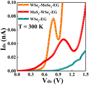
 Current-voltage curves of single junction (green) van der Waals solid (no NDR) and multijunction (red, orange) van der Waals solids (NDR). Stacking and choice of materials determines the location and width of peak. Image: Yuchuan Lin
The researchers observed negative differential resistance (NDR), which is a quantum transport effect, when they applied voltage to one-atom-thick layer structures of van der Waals materials. These structures have three parts, of which the base is graphene. This base has atomic layers of either tungsten diselenide (WSe2) or molybdenum diselenide (MoSe2), molybdenum disulfide (MoS2).
In the NDR quantum transport effect, electrons have a wave nature that enables them to tunnel through any type of material with varying resistance. NDR could be effectively used in high frequency, low voltage electronic circuits.
“Theory suggests that stacking two-dimensional layers of different materials one atop the other can lead to new materials with new phenomena,” said Joshua Robinson, a Penn State assistant professor of materials science and engineering.
Interfaces that are nearly perfect are required for achieving NDR at room temperature in a resonant tunneling diode. Direct growth techniques can be used for achieving these nearly perfect interfaces. WSe2 and MoSe2 can be produced using metal organic chemical vapor deposition, and MoS2 layers can be produced by oxide vaporization of molybdenum oxide along with sulfur vapor.
“This is the first time these vertical heterostructures have been grown like this,” Robinson said. “People typically use exfoliated materials that they stack, but it has been extremely difficult to see this phenomenon with exfoliated layers, because the interfaces are not clean. With direct growth we get pristine interfaces where we see this phenomenon every time.”
When Robinson was conducting the study along with his student Yu-Chuan Lin, they observed a sharp valley and peak in their electrical measurements. Normally, it would have been a standard upward slope. Robinson states that any repeatable unexpected phenomenon holds considerable interest. Suman Datta, a nanoscale electronic devices expert, observed that the phenomenon seen by Robinson and Lin was a resonant tunneling diode’s 2D version. This diode is a low power quantum mechanical device.
“Resonant tunnel diodes are important circuit components,” said Datta, a coauthor on the paper and Penn State professor of electrical engineering. “Resonant tunneling diodes with NDR can be used to build high frequency oscillators. What this means is we have built the world’s thinnest resonant tunneling diode, and it operates at room temperature.”
Robert Wallace, of the University of Texas, a coauthor of the study, stated that this research is a significant achievement in the endeavor to obtain useful 2D integrated circuits.
“The ability to observe the resonant behavior at room temperature with synthesized 2D materials rather than exfoliated, stacked flakes is exciting as it points toward the possibilities for scalable device fabrication methods that are more compatible with industrial interests. The challenge we now must address includes improving the grown 2D materials further and obtaining better performance for future device applications,” Wallace said.
The detailed atomic resolution materials characterization for the Penn State resonant tunneling diodes was done by the coauthors from UT-Dallas.
Ram Krishna Ghosh, a post-doctoral researcher at UT-Dallas, had provided a theoretical understanding about the electron transport that takes place in the 2D layered materials. The experimental results and Ghosh’s calculations were found to have a close correspondence. However, Datta states that in a circuit, the newly developed resonant tunnel diode is just a single component, and other elements including transistors have to be built in 2D.
“The take home message,” he said, “is that this gives us a nugget that we as device and circuit people can start playing around with and build useful circuits for 2D electronics.”
Yu-Chuan Lin is the first author of this study that has been published as a paper titled “Atomically Thin Resonant Tunnel Diodes Built from Synthetic van der Waals Heterostructures,” in the journal Nature Communications.
The other coauthors of this study include Rafik Addou, Hui Zhu, Moon Kim, Ning Lu, and Xin Peng, all at UT-Dallas; Sarah Eichfield at Penn State; Lain-Jong Li, at King Abdullah University of Science and Technology, Saudi Arabia; and Ming-Yang Li at Institute of Atomic and Molecular Sciences, Taiwan.
The Semiconductor Research Corporation and DARPA through the Center for Low Energy Systems Technology have supported this study, which was done in conjunction with the Center for Two-Dimensional and Layered Materials (2DLM) at Penn State. The Nanoelectronics Research Initiative and NIST also provided support for the work done at UT-Dallas.