Sep 14 2016
 Image credit: Anagh Bhaumik.
A method that helps to integrate reduced graphene oxide (rGO), graphene oxide (GO) and graphene onto silicon substrates at room temperature using nanosecond pulsed laser annealing has been developed by materials researchers at North Carolina State University.
This invention increases the possibility of developing new electronic devices, and the researchers have already started to plan the utilization of this new method for producing smart biomedical sensors.
In this new method, researchers commenced with a silicon substrate. The researchers used domain matching epitaxy to top that with a layer of single-crystal titanium nitride and to guarantee aligning of the crystalline structure of the titanium nitride with the silicon’s structure.
A copper-carbon (Cu-2.0atomic percent C) alloy was then placed on top of the titanium nitride, with the help of the domain matching epitaxy. As a final step, the team melted the alloy’s surface with nanosecond laser pulses, which pulls carbon to the surface.
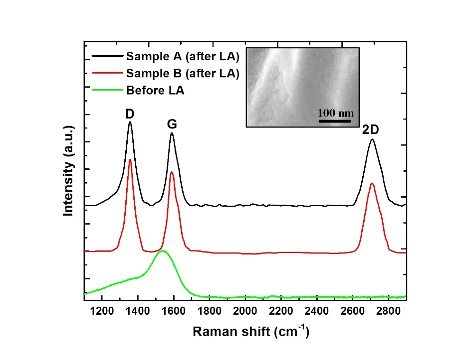
Performing this process in a vacuum will result in the formation of carbon on the surface as graphene. When performed in oxygen, it develops GO, and when carried out in a humid atmosphere followed by a vacuum, it forms as rGO. The carbon’s crystalline structure, in all these scenarios, is aligned with the underlying copper-carbon alloy.
We can control whether the carbon forms one or two monolayers on the surface of the material by manipulating the intensity of the laser and the depth of the melting. The process can easily be scaled up. We’ve made wafers that are two inches square, and could easily make them much larger, using lasers with higher Hertz. And this is all done at room temperature, which drives down the cost.
Jay Narayan, Professor, North Carolina State University
Graphene is considered to be an exceptional conductor, even though it cannot be used as a semiconductor. However, rGO is treated as a semiconductor material capable of being used to develop electronic devices such as optic-electronic devices and integrated smart sensors.
“We have already patented the technique and are planning to use it to develop smart biomedical sensors integrated with computer chips,” Narayan says.
The paper, “Wafer Scale Integration of Reduced Graphene Oxide by Novel Laser Processing at Room Temperature in Air,” was published Sept. 9 in the Journal of Applied Physics. Anagh Bhaumik, a Ph.D. student at NC State, is the lead author of the paper. The National Science Foundation under grant number ECCS-1306400 supported this research.