Mar 31 2017
 Credit: North Carolina State University
A research team at North Carolina State University (NC State) has developed a new method for changing positively charged (p-type) reduced graphene oxide (rGO) into negatively charged (n-type) rGO. The resultant layered material can be employed to develop rGO-based transistors, which can be used in electronic devices.
Graphene is extremely conductive, but is not a semiconductor; graphene oxide has a bandgap like a semiconductor, but does not conduct well at all – so we created rGO. But rGO is p-type, and we needed to find a way to make n-type rGO. And now we have it for next-generation, two-dimensional electronic devices.
Jay Narayan, John C. Fan Distinguished Chair Professor of Materials Science and Engineering, NC State
Narayan and Anagh Bhaumik – a Ph.D. student in his lab – specifically showed two major things in this study.
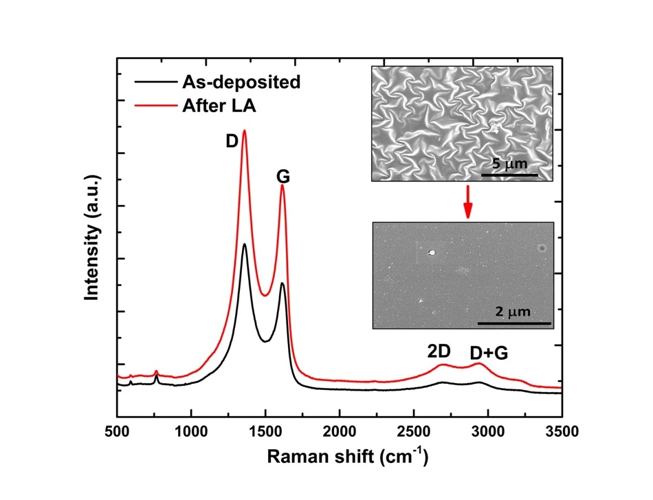
First, they successfully integrated rGO onto silicon and sapphire wafers across the whole wafer. Second, the team disrupted chemical groups by using high-powered laser pulses at regular intervals throughout the wafer. This disruption caused the electrons to move from group to group, thus effectively converting p-type rGO into n-type rGO.
The whole process takes less than one-fifth of a microsecond, and is performed at room pressure and temperature using high-power nanosecond laser pulses.
The laser radiation annealing affords a high degree of depth and spatial control for producing the preferred n-type regions required to create p-n junction-based two-dimensional (2D) electronic devices.
This results in a wafer with a p-type rGO layer underneath and an n-type rGO layer on the surface. This is very important because the p-n junction – the junction where the two types meet – makes the material feasible for transistor applications.
The paper titled, “Conversion of p to n-type Reduced Graphene Oxide by Laser Annealing at Room Temperature and Pressure,” is reported in the Journal of Applied Physics.
Bhaumik is lead author. The National Science Foundation supported the study.