Dec 19 2017
Graphene Flagship scientists, led by researchers at ICFO - The Institute of Photonic Sciences in Barcelona, Spain, have detected graphene’s out-of-plane heat transfer in van der Waals heterostructures. In their paper published in Nature Nanotechnology they follow this process in real-time. This phenomenon has many implications for optoelectronic devices.
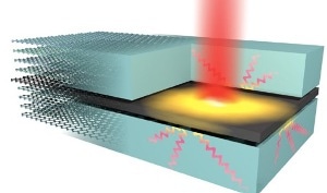
 Schematic representation of the highly efficient out-of-plane heat transfer from graphene hot electrons (yellow glow), created by optical excitation (red beam), to hyperbolic phonon-polaritons in hBN (wave lines). Credit: ICFO
Nanoscale heat flow plays a crucial role in many modern electronic and optoelectronic applications, such as thermal management, photodetection, thermoelectrics and data communication. Layered materials are very promising for many of these applications. Heterostructures consisting of different layered materials stacked one on top of the other open an even wider range of opportunities. These stacks can consist of materials with different physical properties, while the interfaces between them are ultraclean and atomically sharp.
Graphene has a large in-plane thermal conductivity, making it ideal for thermal management of nanoscale devices. The understanding of the out-of-plane heat transfer in heterostructures can help to improve the performance of graphene based electronic and optoelectronic devices.
This was a collaborative research effort within the Graphene Flagship, lead by ICREA Professor Frank Koppens from ICFO - The Institute of Photonic Sciences in Barcelona, Spain and also comprising researchers from Flagship partners in The Netherlands (Radboud University), Italy (Istituto Italiano di Tecnologia – IIT, Consiglio Nazionale delle Ricerche - CNR), Germany (RWTH Aachen University, Max Planck Institute for Polymer Research) and the United Kingdom (The University of Manchester and The University of Cambridge). They observed and followed, in real-time, the way in which heat transport occurs in stacks consisting of graphene encapsulated by the dielectric layered material, hexagonal boron nitride (hBN).
‘Apart from the scientific interest, these findings are also very important for the development of ultra-fast photodetectors.’ Said ICREA Professor Frank Koppens.
The team identified an interesting effect: rather than staying within the graphene sheet, the heat flows to the surrounding hBN. This occurs on an ultrafast timescale of picoseconds (one millionth of a millionth of a second), and is therefore dominant over competing (in-plane) heat transfer processes.
This was found to rely on two interesting phenomena: hot electrons in graphene and hyperbolic phonons in hBN. Graphene makes hot electrons by transferring incident light into electrical heat and it is these hot electrons that interact with the adjacent hBN layer and enable the out-of-plane heat transfer. The process for this involves the coupling of the hot electrons to hyperbolic phonon-polaritons in the hBN sheets which then propagate within the hBN as light does in an optical fiber, but in this case for infrared wavelengths and at the nanometer scale. It turns out that these hyperbolic modes are very efficient at carrying heat away.
‘To study these heat transport phenomena we fabricated a graphene-based photodetector and examined the photoresponse as a function of time delay between two incident light pulses of femtosecond duration. This allowed us to obtain the dynamics of the photoresponse, which indicated carrier cooling on a picosecond timescale. The cooling dynamics exhibited a distinct dependence on graphene carrier density, substrate temperature, hot electron temperature, and – strikingly – hBN sheet thickness. All observations are in quantitative agreement with out-of-plane cooling to hBN hyperbolic phonons as confirmed by theoretical calculations. Based on this understanding of heat transfer, follow-up studies are now aimed at controlling heat transfer.’ said Klaas-Jan Tielrooij from ICFO who is the lead author on the paper.
The results of this work have implications for many applications based on hBN-encapsulated graphene, sometimes referred to as the next generation graphene platform owing to its superior electrical properties. In particular, it will provide direction to optoelectronic device design, where these heat flow processes can be thoroughly exploited.
Professor Andrea C. Ferrari, Science and Technology Officer of the Graphene Flagship, and Chair of its Management Panel, added ‘the combination of graphene and BN is at the moment the most promising to develop future optoelectronic devices, such as modulators and detectors. This work will have implications to implement the Flagship roadmap translating the potential of graphene and related materials for applications in the future 5G communications and the Internet of Things.’