Dec 2 2019
Perovskite nanocrystals show potential for enhancing a broad range of optoelectronic devices, from light-emitting diodes (LEDs) to lasers. However, these materials are not extensively used at the commercial level because of their durability problems.
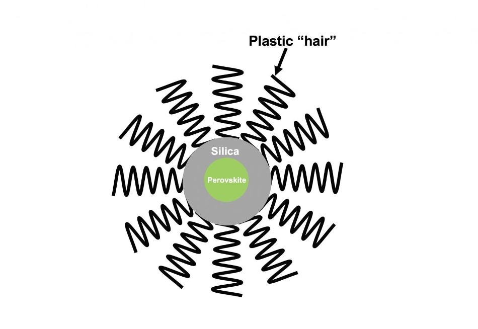
 This illustration shows how the two layers of plastic and silica work together to protect the perovskite material. Image Credit: Georgia Tech.
To deal with the durability problem of the perovskite material, scientists at the Georgia Institute of Technology (Georgia Tech) have described an innovative method in which the perovskite is encased within a double-layer protection system produced from silica and plastic.
The researchers have demonstrated a multistep process to create encased perovskite nanocrystals that do not degrade easily in moist settings. The study has been recently published in the Science Advances journal on November 29th, 2019.
Perovskite nanocrystals are highly susceptible to degradation, particularly when they come into contact with water. This dual-shelled system offers two layers of protection while allowing each nanocrystal to remain a distinct and separate unit, achieving the maximum amount of surface area and other physical characteristics of the perovskite needed for optimizing optoelectronic applications.
Zhiqun Lin, Professor, School of Materials Science and Engineering, Georgia Institute of Technology
Perovskite is a term that refers to the material’s crystal structure. The material is typically made up of three parts—a couple of cations of varying sizes and a single anion in between. For many years, scientists have been trying to replace different types of chemicals into the structure to obtain exclusive properties. Perovskites, in particular, comprising halide compounds such as iodine and bromide can serve as light emitters and absorbers.
For this analysis, Lin’s team tested one of the most standard halide configurations formed from bromide, lead, and methylammonium. The study was supported by the Air Force Office of Scientific Research, the Defense Threat Reduction Agency, the National Science Foundation, and the U.S. Department of Energy.
In the researchers’ process, star-shaped plastic molecules are initially formed that can potentially act as “nanoreactors.” To form these molecules, 21 polymer arms are first grown on a simple sugar molecule. Then, after the plastic molecule is loaded with precursor chemicals for the perovskite nanocrystals and silica, many stages of chemical reactions create the ultimate system.
Once the star-shaped plastic has served as a nanoreactor, the star-shaped components continue to be indefinitely fixed, virtually like hair, to the silica. It is this silica that covers the perovskite. Subsequently, the hairs not only repel water but also prevent the perovskite nanocrystals from clumping together, serving as the initial layer of protection. The subsequent silica layer further protects the nanocrystals in case water enters the water-repelling plastic hairs.
Synthesis and applications of perovskite nanocrystals have been a rapidly evolving research field over the past five years. Our strategy, based on a judiciously designed star-shaped plastic as a nanoreactor, enables unprecedented control in the crafting of high-quality perovskite nanocrystals with complex architecture, which is inaccessible in conventional approaches.
Yanjie He, Study Coauthor and Former Graduate Student, Georgia Institute of Technology
To test the material, the scientists used a thin film of the encapsulated perovskites to coat glass substrates and then carried out a number of stress tests, like soaking the whole sample in deionized water.
When the sample was illuminated with ultraviolet light, the researchers observed that the photoluminescent characteristics of the perovskites did not reduce throughout a 30-minute test. For comparison purposes, the scientists also submerged unencapsulated perovskites in water and observed as their photoluminescence disappeared within a matter of seconds.
According to Lin, the novel technique demonstrates that the surface properties of the dual-shelled nanocrystal could be altered to improve its performance in a broader range of applications. Also, the process of using star-shaped plastic to fabricate the novel perovskite nanocrystals plastic was unusual because only low-boiling-point solvents with reduced toxicity were used.
Upcoming studies may focus on producing different perovskite nanocrystal systems, such as doped perovskites, double perovskites, and all-inorganic perovskites.
We envision that this type of perovskite nanocrystal will prove very useful for creating durable optoelectronic devices for bioimaging, biosensors, photonic sensors, and radiation detection, as well as next-generation LEDs, lasers, and scintillators. This is because these hairy perovskite nanocrystals carry unique advantages, including high defect tolerance, narrower emission bands, and high scintillation efficiency.
Zhiqun Lin, Professor, School of Materials Science and Engineering, Georgia Institute of Technology
The study was supported by the National Science Foundation (NSF) under grant Nos. CMMI 1727313, CMMI 1914713, CBET 1803495, the Defense Threat Reduction Agency under grant No. HDTRA1-18-1-0004, Air Force Office of Scientific Research under grant No. FA9550-19-1-0317, and the U.S. Department of Energy under grant Nos. DE-SC0018611 and DE-FG02-90ER46604.
Perovskite Protection System
The new protection system can help perovskite LEDs withstand water. Video Credit: Josh Brown.