Feb 11 2020
Electronic cloth and wearable tech could be the path forward. However, to reach there, it is essential for the wiring to be flexible, strong, and efficient.
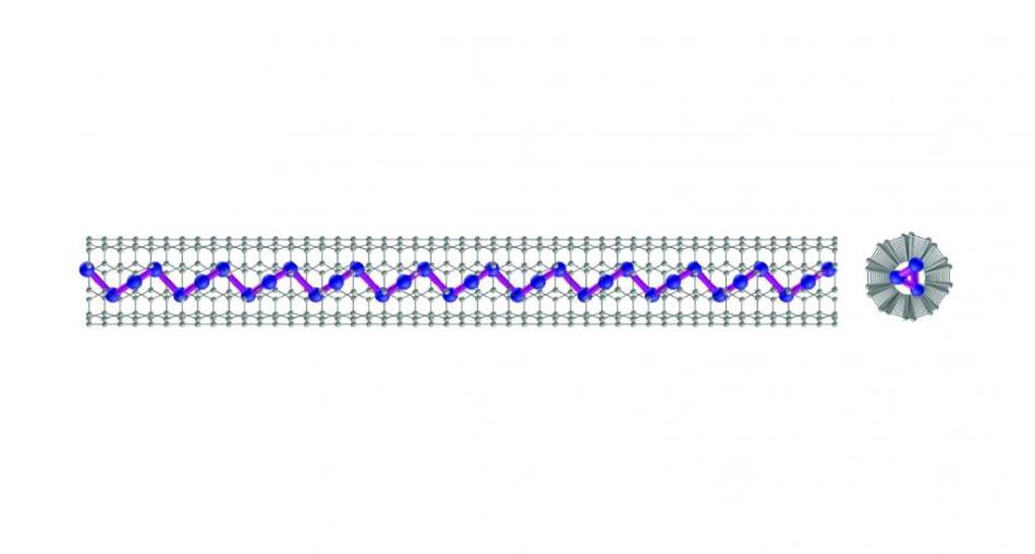
 Researchers have discovered that a material forms a DNA-like helix when reduced to a string of atoms encapsulated in a nanotube and mounted on a metal base. Image Credit: Purdue University/Pai-Ying Liao.
Physicists from Michigan Technological University investigated boron nitride nanotubes (BNNT), that encompass tellurium atomic chains similar to a straw, which can be controlled by pressure and light. They partnered with scientists at Purdue University, Washington University, and the University of Texas at Dallas on the study. The study outcomes were recently reported in Nature Electronics.
With the increase in demand for smaller and faster devices, engineers and researchers opt for materials with properties that can perform well when current materials lose their performance or cannot shrink adequately.
Scientists have started tweaking the atomic structures of nanomaterials for electronic cloth, wearable tech, or very thin devices that can be attached to the surface of tables, cups, space suits, and other materials.
The materials examined by the researchers must bend when a person moves. However, they must not snap or become noodly; moreover, they must withstand different temperatures and still allow enough room to run the software functions expected by users out of their phones and desktops. With preliminary or current technology, this cannot be achieved.
Boron Nitride Nanotubes
By investigating nanoparticles and nanotubes, Yoke Khin Yap has discovered the quirks and potentials of their quantum mechanical behaviors. He pioneered the use of electrically insulating nanotubes for electronics by depositing iron and gold nanoparticles on the surface of boron nitride nanotubes (BNNTs).
The quantum tunneling of the material was improved by the metal-nanotube structures by behaving like atomic steppingstones that could assist electronics to get out of the confines of silicon transistors, which power a majority of the existing devices.
In the recent past, Yap's team also developed atomically thin gold clusters on BNNTs. As suggested by the “tube” of their nanostructure, BNNTs are hollow in the middle. They are very good insulators and as flexible and strong as an Olympic gymnast.
Due to these features, they have been regarded as a good candidate to couple with tellurium—another material that holds immense electrical potential. Tellurium atomic chains turn into a small wire with high current-carrying capacity upon stringing them into atom-thick chains, which are very thin nanowires, and threading them through the BNNTs’ hollow center.
Without this insulating jacket, we wouldn’t be able to isolate the signals from the atomic chains. Now we have the chance to review their quantum behavior. This is the first time anyone has created a so-called encapsulated atomic chain where you can actually measure them. Our next challenge is to make the boron nitride nanotubes even smaller.
Yoke Khin Yap, Physicist, Michigan Technological University
Atomic Chains of Tellurium
A bare nanowire is similar to a loose cannon. It is very challenging to control its electric behavior—or even just gaining insights into it—when it is in uncontrolled contact with flyaway electrons.
Tellurium is a metalloid analogous to sulfur and selenium, and its nanowires are anticipated to exhibit various electronic and physical properties compared to bulk tellurium. Scientists just required a way to segregate it, which can now be provided by the BNNTs.
This tellurium material is really unique. It builds a functional transistor with the potential to be the smallest in the world. Silicon atoms look straight, but these tellurium atoms are like a snake. This is a very original kind of structure.
Peide Ye, Lead Researcher, Purdue University
Ye explained that the researchers were fascinated to find that the atoms in these one-dimensional chains wiggled. They observed this using transmission electron microscopy at the University of Texas at Dallas.
Using the tellurium-BNNT nanowires, field-effect transistors with a width of just 2 nm were created, while silicon transistors existing on the market have a width of 10–20 nm. The current-carrying capacity of the new nanowires reached 1.5 × 10⁸ A cm−2, which also surpasses the capacity of a majority of the semiconducting nanowires.
Upon encapsulating, the researchers evaluated the number of tellurium atomic chains contained within the nanotube and analyzed single and triple bundles distributed in a hexagonal pattern. Moreover, tellurium-filled nanowires respond quickly to pressure and light, which is another potential feature for future electronics.
The tellurium nanowires were also encapsulated in carbon nanotubes by the researchers, though it is not possible to measure their properties because of the semiconducting or conducting nature of carbon.
Although the team has been able to capture tellurium nanowires inside BNNTs, a large part of the mystery is still unanswered. It is vital to characterize the nature of these atomic chains before their full potential for electronic cloth and wearable tech can be achieved.