Apr 21 2020
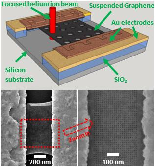
At the Japan Advanced Institute of Science and Technology (JAIST), scientists have been successful in fabricating the suspended graphene nanomesh in a wide area using helium-ion beam microscopy.
 Graphene nanomesh. Image Credit: Hiroshi Mizuta, JAIST.
Nanopores with a diameter of 6 nm were patterned evenly on the 500 nm wide and 1.2 µm long suspended graphene.
A range of stable graphene nanomesh devices was created by systematically manipulating the pitch (from the center of one nanopore to that of another) from 15 nm to 50 nm. This offers a viable method to examine the intrinsic properties of graphene nanomesh for applications such as quantum technology, phonon engineering, and gas sensing.
Graphene has outstanding optical, thermal, and electrical properties. It is a potential candidate for several applications in the next 10 years. Also, graphene is considered to be promising than silicon to develop the next generation of electrical circuits.
But without a bandgap, it is not easy to use graphene as field-effect transistors (FETs). The scientists made attempts to cut the graphene sheet into a small piece of graphene nanoribbon and were also successful in observing the bandgap opening.
However, the current produced by the graphene nanoribbons is insufficient to power the integrated circuit. Therefore, the graphene nanomesh is earmarked by forming periodical nanopores on the graphene, which is also regarded as a tiny graphene nanoribbon array.
Under the guidance of Dr Fayong Liu and Professor Hiroshi MIZUTA, as well as in collaboration with scientists at the National Institute of Advanced Industrial Science and Technology (AIST), a research group has shown that large area suspended graphene nanomesh can be rapidly achieved using helium ion beam microscopy with well-controlled pitches and sub-10 nm nanopore diameter.
The helium-ion beam milling method addresses the speed limitation, when compared to the slow speed TEM patterning, and also offers a high-imaging resolution. Preliminary electrical measurements revealed that there was an exponential increase in the thermal activation energy of the graphene nanomesh when its porosity was increased.
Thus, this process offers a novel technique for bandgap engineering over the traditional nanoribbon technique. The researchers intend to keep investigating graphene nanomesh for phonon engineering applications.
Graphene nanomesh is a kind of new ‘brick’ for modern micromachine systems. Theoretically, we can generate many kinds of periodical patterns on the original suspended graphene, which tunes the property of the device to the direction for a special application, in particular nanoscale thermal management.
Hiroshi Mizuta, Professor and Head of MIZUTA Laboratory, Japan Advanced Institute of Science and Technology
At present, the MIZUTA laboratory is designing the thermal and electrical properties of graphene-based devices for basic physics and prospective applications like thermal rectifier and gas sensors. The ultimate goal of the researchers is to build a green world by using graphene.
This study was funded by the Grant in Aid for Scientific Research No. 18H03861, 19H05520, from the Japan Society for the Promotion of Science (JSPS).