A group of scientists from Oxford University’s Department of Materials headed by Harish Bhaskaran, Professor of Applied Nanomaterials, present a novel strategy of picking up single nanowires from the growing substrate and placing them on nearly any platform with sub-micron accuracy. This breakthrough could expedite the creation of ever smaller and more sophisticated computer chips.

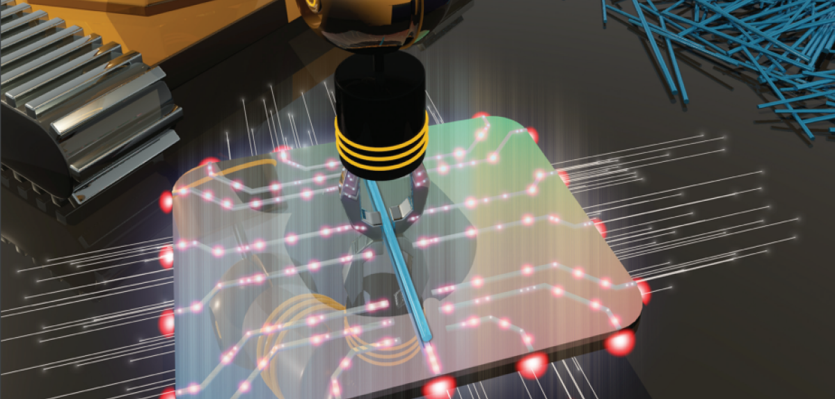
A new method developed by Oxford researchers enables nanowires to be placed precisely onto chip devices. Image Credit: Small, Wiley.
The breakthrough method employs novel tools, such as ultra-thin PET filaments with tapered nanoscale tips that are utilized to pick up individual nanowires. Adhesive van der Waals forces (small forces of attraction between atoms and molecules) allow the nanowires to “jump” into contact with the tips at this fine scale.
The nanowires are subsequently applied to a glass slide by a transparent dome-shaped elastic stamp. The stamp is then turned upside down and aligned with the device chip, and the nanowire is softly printed onto the surface.
The nanowires that were deposited had strong adhesive properties, staying in place even after the device was submerged in liquid. The scientists were also able to install nanowires on delicate substrates like ultra-thin 50 nanometer membranes, illustrating the stamping technique’s sensitivity and adaptability.
Furthermore, the approach was employed to create an optomechanical sensor, which is a device that employs laser light to monitor vibrations, that was 20 times more sensitive than current nanowire-based devices.
Nanowires, materials with 1000 times the diameter of a human hair and intriguing physical properties, allow major advances in a wide range of sectors, from energy harvesters and sensors to information and quantum technologies.
Their microscopic size, in particular, may enable the development of smaller transistors and miniaturized computer chips. However, one significant obstacle to realizing nanowires’ complete potential has been their inability to be precisely positioned within devices.
The conditions required to manufacture nanowires are too extreme for most electronic device production procedures. As a result, nanowires are often grown on a separate substrate before being mechanically or chemically relocated to the device. However, in all available nanowire transfer procedures, the nanowires are randomly deposited on the chip surface, limiting their use in commercial products.
This new pick-and-place assembly process has enabled us to create first-of-its-kind devices in the nanowire realm. We believe that it will inexpensively advance nanowire research by allowing users to incorporate nanowires with existing on-chip platforms, be it electronic or photonic, unlocking physical properties that have not been attainable so far.
Utku Emre Ali, D.Phil. Student, Department of Materials, University of Oxford
Utku Emre Ali, who devised the technique, adds, “Furthermore, this technique could be fully automated, making full-scale fabrication of high quality nanowire-integrated chips a real possibility.”
This technique is readily scalable to larger areas, and brings the promise of nanowires to devices made on any substrate and using any process. This is what makes this technique so powerful.
Harish Bhaskaran, Professor, Department of Materials, University of Oxford
The research was financially supported by EPSRC via the Fellowships in Manufacturing (Grant no. EP/R001677/1).
Journal Reference:
Ali, U. E., et al. (2022) A Universal Pick-and-Place Assembly for Nanowires. Small. doi.org/10.1002/smll.202201968.