The precise arrangement of nanoparticles on arbitrary surfaces is highly desirable for leveraging their distinct properties in the preparation of highly functional nanoscale devices. However, realizing such surfaces is challenging.

Study: Nanoparticle contact printing with interfacial engineering for deterministic integration into functional structures. Image Credit: Anna Kireieva/Shutterstock.com
Recent research published in Science Advances proposed a robust method to address this challenge, where a topographical template with spatially arranged nanoparticles was printed onto different surfaces via a single contact-and-release step. This technique showed a transfer yield of >95% and a placement accuracy of <50 nanometers.
Unlike conventional methods, the proposed approach was devoid of mediation steps, which otherwise require solvents or polymer sacrificial layers. Moreover, avoiding mediation steps controlled any damage or contamination to the surface, making their integration into functional structures a possible affair.
Furthermore, the possibility of integration of these surfaces into functional structures was examined using a particle-on-mirror model system, where more than 2000 systematically defined nanocavities exhibited a coherent plasmonic response with negligible interstructure variability.

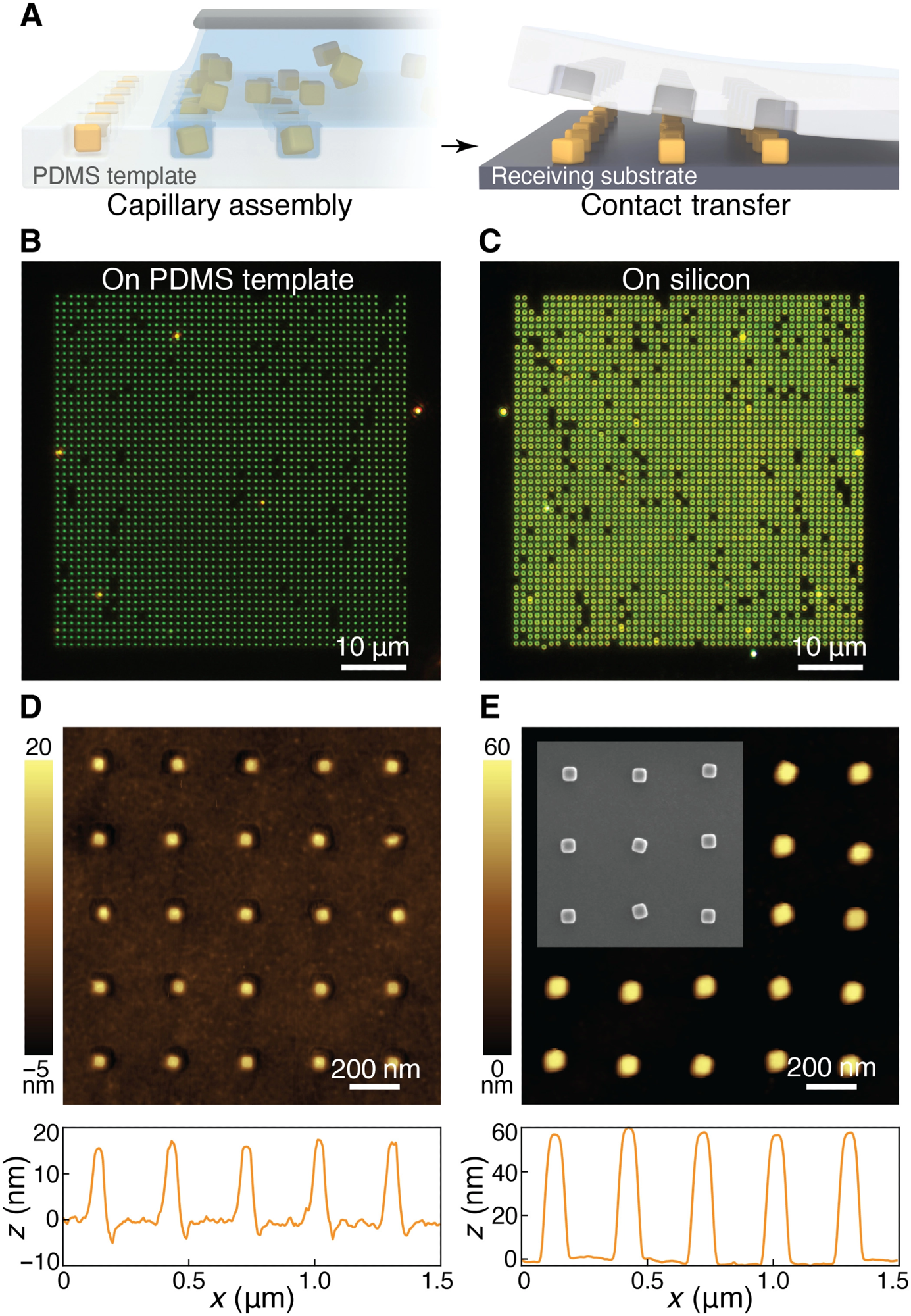
Nanoparticle contact printing for precise, scalable, and pristine particle patterning. (A) Schematic of the printing process: Nanoparticles are positioned onto a PDMS topographical template using capillary assembly, followed by their dry contact transfer onto a receiving substrate. (B) Dark-field image of a representative 50 × 50 array of ~55-nm gold nanocubes assembled onto a PDMS template. (C) Dark-field image of the same nanocube array after contact transfer onto a silicon substrate. (D) AFM image of gold nanocubes assembled onto PDMS template with the height profile showing particle protrusion above the template surface. (E) AFM image and height profile after transfer onto silicon surface. The inset shows a scanning electron microscope (SEM) image of the corresponding cubes at the same scale. Image Credit: Zhu, W et al., Science Advances
Bottom-Up Process for Building Nanoparticles
Conventionally, nanoscale devices are commonly built from the top down, where the materials are etched to achieve the preferred nanostructure arrangement. However, developing the smallest nanostructures with superior performance and novel functionalities necessitates expensive equipment.
On the other hand, bottom-up synthesis efficiently produces nanoparticles with tailored compositions, structures, and functionalization that outperforms their top-down manufactured counterparts. Here, individual particles must be incorporated into deterministic designs to leverage their emergent properties in functional nanodevices.
Various assembly methods have been developed to achieve this goal, in which external factors or local physical and chemical signals guide the accurate particle placement. Examples of such assemblies include magnetic, optical, electrostatic trapping, capillary assembly, dielectrophoretic positioning, and DNA-mediated patterning.
Nevertheless, these techniques are incongruent with arbitrary systems and frequently lack high-throughput processing because they rely on specific particle characteristics and surface treatments.

Improving transfer yield with interfacial engineering. (A) Single-particle transfer yield as a function of transfer temperature. (B) Single-particle transfer yield as a function of the particle protrusion height (h), at a transfer temperature (T) of 75°C. (C) Transfer yield of multiparticle linear structures as a function of the number of constituent nanoparticles at room temperature (purple) and at 75°C (orange). The error bars represent intrasample variations in transfer yields measured for 50-μm by 50-μm arrays of individual nanoparticles across millimeter-scale areas of the sample. Image Credit: Zhu, W et al., Science Advances
Another concern is interfacing with the underlying surface for device integration because damage, surface modification, and contamination are often unavoidable in these techniques. As a result, a robust method for scalable and accurate patterning of nanoparticles into varied and pristine structures over large regions is highly desirable.
Engineers have previously grown nanoparticles in solution, then poured the solution onto a template, organized the nanoparticles, and moved them to the surface. However, this technique is challenging to perform, and transferring them to a surface typically necessitates the use of high pressure, chemical glue, or elevated temperatures, which can alter and damage the surface of the prepared device.
Moreover, when nanoparticles are in liquid, capillary forces dominate, and van der Waals forces dominate at the interface between the nanoparticles and the solid surface with which they come into contact.
When a drop of liquid is dragged across the template, capillary forces move the nanoparticles into the desired trap, precisely positioning them. When the liquid dries, van der Waals forces keep the nanoparticles in place.
Highlighting the nature of capillary forces and the contribution through present work, Zhu, one of the authors of this study, mentioned in a recent press release "These (capillary) forces are ubiquitous and can often be detrimental when it comes to the fabrication of nanoscale objects as they can cause the collapse of the structures. But we are able to come up with ways to control these forces very precisely to use them to control how things are manipulated at the nanoscale".
Nanoparticle Contact Printing with Interfacial Engineering
In the present study, a two-step method, nanoparticle contact printing, was proposed to prepare nanoparticles of a defined size and shape in a solution. Initially, the processing flexibility of the capillary assembly helped to realize single-particle spatial ordering.
Here, the capillary forces, which were unaffected by the particle type, immobilized the nanoparticles into spatially defined target sites. Although capillary assembly promoted the positioning of various materials, it did not facilitate their facile integration into operational systems.
The wet processing used in this technique introduced contaminants into the receiving surfaces. Furthermore, after positioning, the assembled particles were partially integrated into the template, restricting their integration into the active systems.
Although the polymeric template’s thermal removal destroyed the contact between the particles and the template, the elevated temperatures hindered their applications involving temperature-sensitive nanoparticles or substrates.

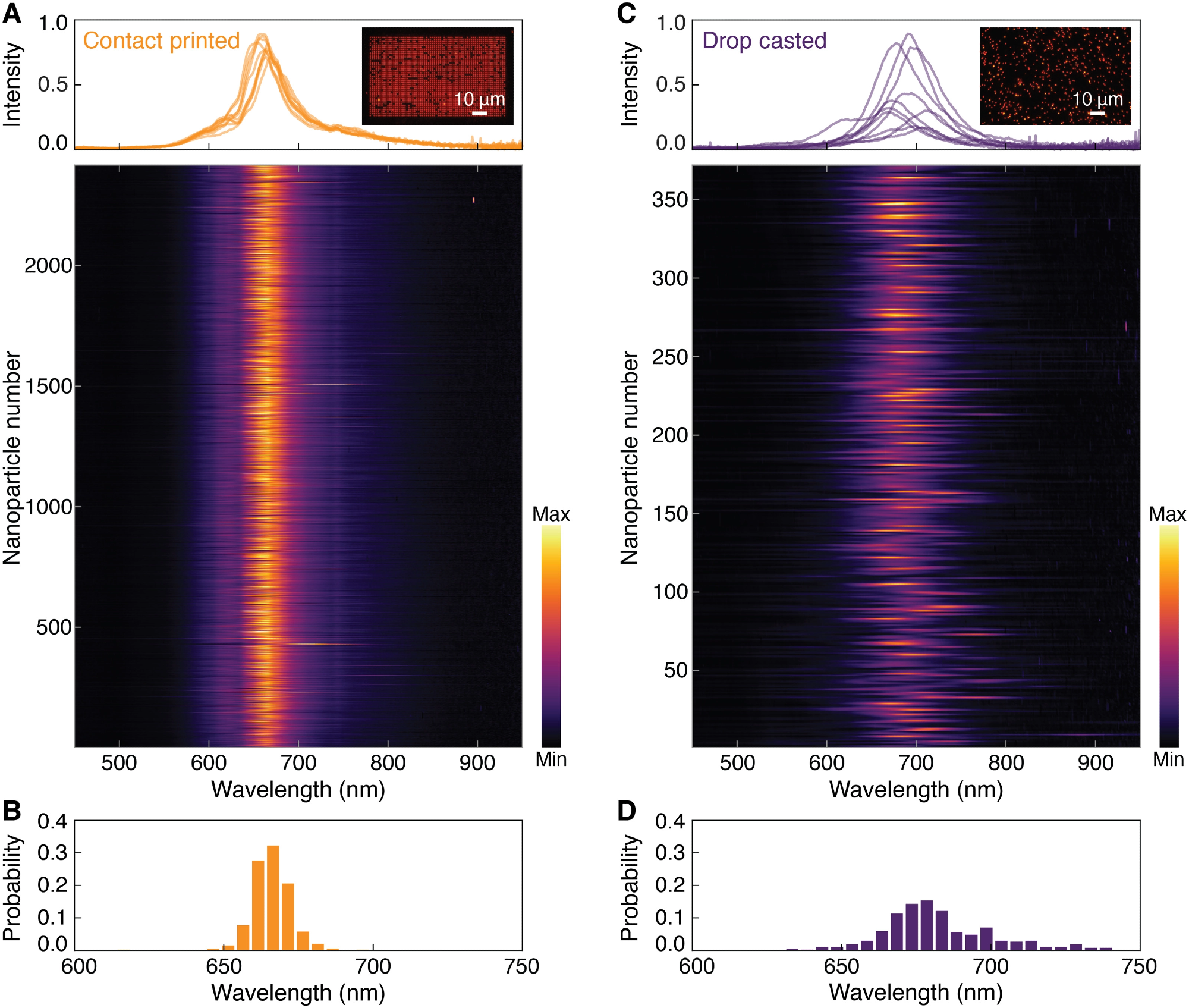
Uniform spectral response in a contact-printed particle-on-mirror nanocavity array. (A and B) Contact-printed NPoM nanocavities are compared against (C and D) the drop-casted structures. For each case, 10 random single-particle spectra are shown on the top plot, with dark-field image as inset. Dark-field scattering spectra of all sampled nanocubes are shown in the waterfall plots. A tighter resonance peak distribution is observed for (B) 2417 contacted-printed nanoparticles (666 ± 8 nm), as compared to (D) 371 drop-casted particles (681 ± 22 nm). Image Credit: Zhu, W et al., Science Advances
The subsequent transfer of the nanoparticles was driven by their interfacial interactions with the target. However, owing to the lack of conformal contact and nanoscale dimensions, the adhesive interactions between individual nanoparticles are insufficiently small, resulting in low and uncertain transfer yields.
Thus, modulating the interfacial interactions of the nanoparticles with the template and substrate helped realize efficient transfer via single-step dry contact and release. Thus, the versatility of the capillary assembly and transfer printing steps allowed the present technique to support a wide range of material systems.
Thus, highlighting the significance of the present work, another author of this study, Farnaz Niroui, mentioned, "By integrating these building blocks with other nanostructures and materials we can then achieve devices with unique functionalities that would not be readily feasible to make if we were to use the conventional top-down fabrication strategies alone."
Conclusion
In summary, a robust technique was developed for accurate and optimizable nanoparticle arrangement with single-particle resolution. This approach was based on engineering interfacial interactions at the nanoscale level, facilitating the printing of capillary-assembled particles on a broad range of surfaces without surface treatments, solvent requirements, or sacrificial release layers.
Unlike conventional nanoparticle arrangement strategies, this approach retained the inherent particle properties, and surfaces were maintained contaminant-free during patterning, resulting in suitable interfaces for their integration into functional nanoscale devices.
The fabricated structures were achieved with high throughput and negligible variability, resulting in a uniform and predictable performance, as demonstrated by a sensitive plasmonic nanoparticle-on-mirror design.
Reference
Zhu, W., Satterthwaite, P.F., Jastrzebska-Perfect, P., Brenes, R., Niroui, F. (2022). Nanoparticle contact printing with interfacial engineering for deterministic integration into functional structures. Science Advances. https://doi.org/10.1126/sciadv.abq4869.
Disclaimer: The views expressed here are those of the author expressed in their private capacity and do not necessarily represent the views of AZoM.com Limited T/A AZoNetwork the owner and operator of this website. This disclaimer forms part of the Terms and conditions of use of this website.