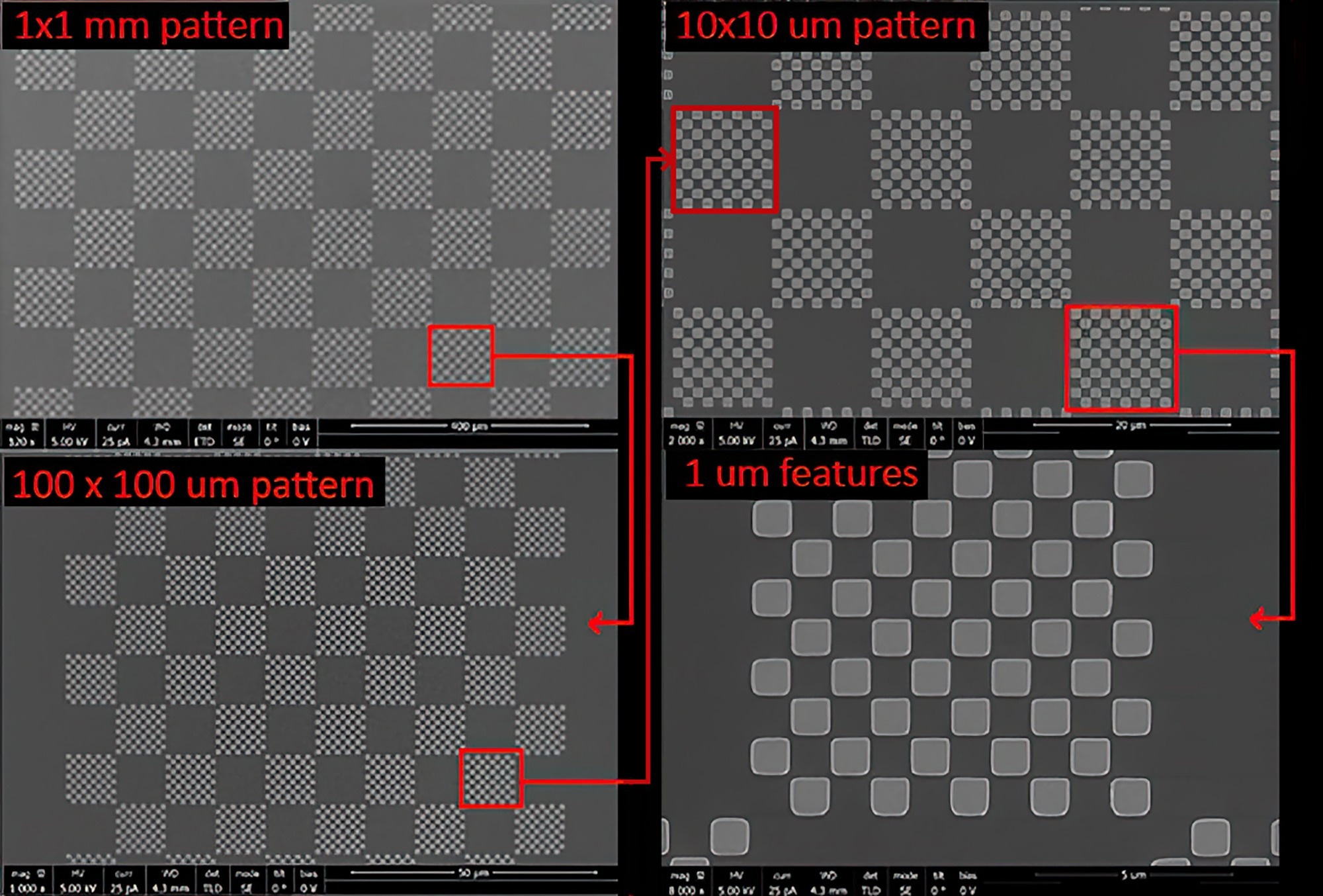
Micro to Nano has introduced the EM-Tec Checkerboard calibration standard, which is designed for quick and easy magnification and image calibration of SEMs. It consists of over 1.6 million squares which form four stages of checkerboard patterns. The smallest checkerboard is 10 x 10 um, which in turn form a pattern of 100 x 100 um and these again form checkerboards of 1 x 1 mm. The 1 x 1mm checkerboards then form a 5 x 5 mm pattern.

Image Credit: Labtech
The smallest 1 x 1 um squares are made of 20nm thick chromium and 40nm gold-on-chromium, deposited on an ultra-flat, conductive, boron-doped <100> silicon substrate. These materials are considered inert under normal working conditions. Imaging contrast is good for both SE and BSE imaging, especially at lower keV. Checkerboard is suitable for SEM magnification calibration in the range of 20x to 50,000x with a pitch accuracy of ± 0.1% in both X and Y directions. It is also useful for checking image distortions and the accuracy of motorized SEM stages.
EM-Tec Checkerboard calibration standard is NIST-traceable, with an example of wafer-level certificate of traceability supplied with each EM-Tec Checkerboard calibration standard.
Sussex-based Labtech International offer Checkerboard and an extensive range of Micro to Nano EM, AFM and LM preparation and imaging products in the UK.