Jul 8 2008
With its announcement today of the Magellan™ Family, FEI Company introduced a new class of instruments called extreme high-resolution scanning electron microscopes (XHR SEMs). The Magellan XHR SEM allows scientists and engineers to quickly see things they could not see before, such as 3D surface images at many different angles and at resolutions below one nanometer (about the size of ten hydrogen atoms, side-by-side). Most importantly, the Magellan XHR SEM images samples at very low beam energies, avoiding distortions otherwise caused by the beam penetrating into the material below.
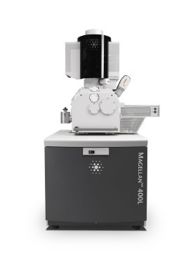
 The extreme high-resolution scanning electron microscopes (XHR SEMs) from FEI.
“The Magellan XHR SEM is the most significant electron optics innovation since FEI introduced the Titan™ Family three years ago,” said Dr. Rob Fastenau, FEI’s executive vice president, marketing and technology. “Magellan is in a class by itself, just as Titan is for transmission electron microscopes, and our innovative Helios NanoLab™ family is for DualBeam™ systems. Magellan is the only family of instruments to make sub-nanometer resolution accessible in a practical sense to non-experts and without restriction on samples—constraints that have previously limited the utility and acceptance of other systems. As the performance benchmark in its category, Magellan is another demonstration of FEI’s deep commitment to being the leading innovator of high-performance solutions in all of our markets.”
Sub-nanometer resolution has critical value in scientific research and industrial R&D. In addition, it is an absolute requirement in process development, monitoring and control applications in advanced semiconductor manufacturing. The Magellan Family extends this capability to applications that were previously impossible or impractical with conventional SEM, transmission electron microscope (TEM) or focused ion beam (FIB) systems.
For example, the ability to provide sub-nanometer resolution over a broad range of beam energies, from less than one kilovolt (kV) to 30kV, allows semiconductor manufacturers to see critical detail on complex three-dimensional structures in 32nm nodes and below, with unprecedented clarity and contrast. Researchers in materials science will now have the ability to generate high-resolution, surface-sensitive images of carbon nanotubes, nanowires and catalysts without the image distortions caused by electrical charging from higher energy electron beams. Across the board, the Magellan Family extends the range of nanoscale imaging and analysis, with the speed and ease-of-use of traditional SEMs.
The Magellan Family’s performance derives from the integration of new electron optical elements, proprietary electron gun technology, a highly accurate five-axis piezo-ceramic stage and high stability platform with fully configurable analytical chamber. The stage readily accommodates large samples or multiple smaller samples, while providing fast, accurate navigation and unequaled stability.
The Magellan Family comes in two models: The Magellan 400 is optimized for scientific research while the Magellan 400L is optimized for semiconductor labs. The semiconductor lab model comes with a load-lock feature that speeds-up sample throughput, and includes a retractable solid state backscatter electron detector (SSBSED) and S2 compliance kit. Both models have an optional, full environmental enclosure to isolate the instrument from thermal and acoustic interferences, ensuring peak performance while relaxing site requirements and facility preparation costs. The Magellan Family is available for purchase now, with initial shipments planned to begin in September 2008.