Jan 18 2009
Structured Materials Industries, Inc. (SMI) announces today that it has opened its application lab facilities for the MOCVD growth of ZnO based films for transparent contact work as used with LEDs and photovoltaics, as well as ZnO films for transparent and power transistors.
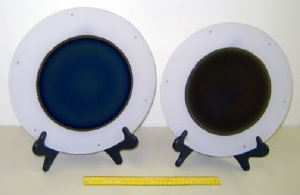
 SMI MOCVD grown ZnO thin films (conductive or insulating) through 8" now routinely produced with less than 3% uniformity
SMI has a decades-long history in development of Zinc Oxide and its alloys and has built considerable capabilities in its in-house applications lab, including 4 ZnO deposition tools, thermal and laser annealing stations, and other support services. These tools are used predominantly in support of customer development needs and deposition tool purchasers.
Our in-house tools include platters are sized at 5" through 12". Materials properties include n-type conductors doped to 10E20 with conductivities as low as ~5E-4 ohm-cm or insulating films at greater than 10E7 ohm-cm. We have experience with a wide range of dopants to tune band gap, index of refraction and conductivity. P-type exploration services are also available.
Our deposition services include demonstrated development of alloys of ZnO (Cd, Mg, Se, Te, and S), doping of ZnO (In, Ga, Al, B, N, P, As, Li, Na, K, and Sb among others) and phosphor or spin materials compositions (Cu, Fe, Co, Mn, Si, Ge, Er, Nb, Eu, and Tb, among others).
Application areas include GaN LEDs, especially UV LEDs, where only ZnO alloys will effectively allow UV light out while maintaining conductivity. ZnO allows effective engineering of the index of refraction, the bandgap, band alignment, and so on. ZnO conductors are applicable to CdTe and CIGS photovoltaics as well as conventional LEDs. ZnO nanowire structures are have great potential as sensors and possibly even a new type of laser. ZnO is highly applicable to thin film transparent and power transistors - at relatively very low cost. ZnO itself - or its alloys - can be used as a phosphor layer in a device structure, such as a white light LED.