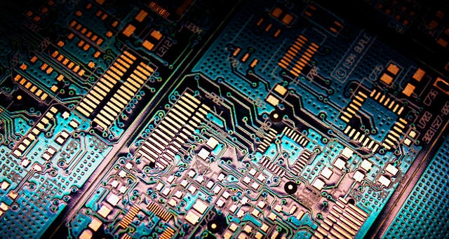
Rice University researchers have created a proof-of-concept prototype for a new type of memory chip based on cheap silicon oxide.

Electronics are getting ever smaller, driven by the demands of Moore's Law. Memory systems based on new materials are vital to allowing futher increases in performance and efficiency as the demands we make on our devices reach the limits of current technology.
The device is a rewritable 1 kilobit memory chip - whilst this is tiny by todays standard, the technology shows promise to one day surpass flash memory in terms of data storage density, energy consumption, and speed.
Silicon nanowire memory
The chip uses a novel architecture developed earlier by the same team - Professor James Tour's research group at Rice University. They discovered that by simply passing a current through a thin layer of silicon oxide, it is possible to strip the oxygen away, leaving a tiny channel of pure conducting silicon just 5 nanometers wide.
By applying voltages to the material, these silicon nanowires can be healed and re-created many times over. Tiny reading currents can then be used to determine whether the channel is open or closed - creating the 0's and 1's necessary to store digital information.
Difficult to develop - easy to manufacture
The channels in the prototype chip were not as small as 5 nanometers - in fact, they were on the scale of a few micrometers. This was done to make fabrication and testing of the device simpler. Prof. Tour commented:
“We didn’t try to miniaturize the device at this stage. We’ve already demonstrated the native sub-5-nanometer filament, which is going to work with the smallest line size industry can make… It will be industry’s job to scale this into commercial memories, but this demonstration shows it can be done.”
The silicon oxide switches were sandwiched in layers of palladium, on top of a layer of aluminium. These layered strips in turn sit on top of a base layer of dopes silicon in a crossbar structure. The aluminium/silicon contacts act as diodes, which help to reduce crosstalk between the memory cells, preventing data corruption.
Testing in space
The demo chip has stood up to laboratory tests so far.
To see how the technology fares outside the lab, earlier prototypes have been shipped to the International Space Station for tests in more extreme environments. One of the key tests for the silicon memory will be how well it maintains data integrity when exposed to the intense radiation of space.
This device is a major hurdle along the way to commercial use of the technology. The ability to scale down to 10nm or even 5nm features will be welcomed by the industry players trying to keep up with Moore's Law, as existing technologies like flash memory simply do not work on such tiny scales.
Sources: