Increasing emphasis on fuel economy requires electrification of the vehicle powertrain, supported by the use of new power semiconductor devices devoted to automotive applications. Currently available electric vehicle systems depend exclusively on silicon-based power management, however, silicon power devices are rapidly approaching maturity, and their performances are restricted to address new requirements of all electric propulsion systems including: high-current (200 to 600 A), high-voltage (100 to 600 V) and low-loss power semiconductor switches. Furthermore, additional improvements on silicon are incremental, while the cost of advancements is increasingly uneconomical.
Gallium Nitride
Next generation electric vehicles require game changing power management solutions with majorly higher efficiency and differentiating system-level advantages compared to existing systems. Thus, new electronic materials and device structures are required. Gallium Nitride (GaN) switches are projected to have a 100x performance advantage over silicon-based devices, because of their exceptional material properties such as high breakdown field, high electron mobility, and high electron velocity. Recent progress in GaN epitaxial growth technology allows the manufacturing of GaN-on-Si wafers with superior quality, large wafer size, and low cost. Due to its compatibility with high-volume silicon fabs, it is possible to manufacture the GaN-on-Si technology platform in large volume, resulting in reduced system cost and superior performance, making this technology a true game changer for automotive applications.
Cathodoluminescence
Cathodoluminescence is one of the main techniques used in semiconductor physics. It is capable of providing characterization of III-V thin film materials with a spatial resolution compatible with the size of the devices, paving the way for an extensive field of research. The Attolight CL system, because of its innovative configuration, offers the following benefits:
- Highly stable cryostage permitting high resolution measurement at 10 K giving information of spatial distribution of defects in order to monitor material doping for example.
- Hyperspectral mapping with acquisition speed well-matched with a good spatial resolution, leading to complete structure characterization on polished cross section.
- High field of view that allows the quantification of threading dislocation defect (TDD) by surface defect mapping.

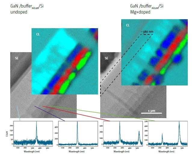
Sample: GaN/Al0.25Ga0.75N/Al0.5Ga0.5N / Al0.8Ga0.2N/AlN/Si polished cross section before and alter Mg+ implantation for GaN p type doping. SEM and CL hyperspectral image treated with classical least square fitting procedure using a set of reference component spectra. Mg doped sample show a low intensity luminescence zone due to defect of Mg implantation.

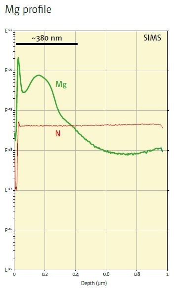
SIMS profiles obtained on the same implanted sample. Depth of defect zone detected by CL is matching the depth detected on SIMS profile.

This information has been sourced, reviewed and adapted from materials provided by Attolight.
For more information on this source, please visit Attolight.