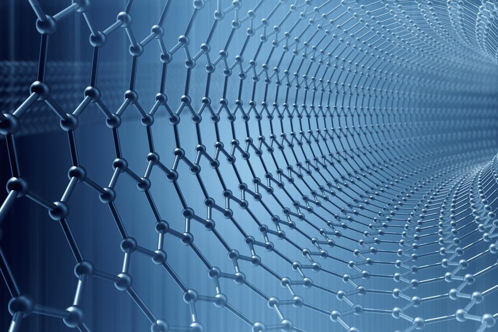
Image Credit: Rost9/Shutterstock.com
Comprised of a single layer of germanium atoms, germanene has recently drawn tremendous interest both in commercial and academic research due to its exceptional potential to be integrated with other modern nanotechnology. This unique material holds promise for the semiconductor industry because of its remarkable magnetic, electronic, and thermoelectric attributes.
In many ways, germanene is similar to graphene, another material made from a single layer of (carbon) atoms. However, unlike the planar atomic lattice of graphene, germanene has a buckled lattice made of two vertically staggered sub-lattices. The comparatively heavy mass, irregular topology, relatively low reactivity, and other key features of germanene make it a promising prospect for flexible electronics, quantum computation, spintronics, and other state-of-the-art applications.
Much of the research to date has focused on the electronic and structural qualities of monolayer germanene, specifically its mechanical and thermal qualities. However, some germanene research has demonstrated that creating interlayer covalent bonds linking two germanene monolayers opens the door to all kinds of potential applications.
Characterizing the Qualities of Germanene Nanoribbons
In one recent study, researchers used molecular dynamics simulations to show the mechanical strength, melting point, and thermal conductivity of both single-layer and bilayer germanene nanoribbons.
The study models estimated the room-temperature thermal conductivity of both kinds of nanoribbon. The models showed that both conductivities are significantly lower than similar nanomaterials. The study also revealed increasing temperature leads to a reduction in the thermal conductivity of both single-layer and bilayer germanene nanoribbons.
In addition, the study team found biaxial tension may improve the thermal conductivity of single-layer nanoribbons, while biaxial compression was found to significantly lower conductivity. When biaxial tension was applied, a blue shift in the adsorption spectrum was observed. When biaxial compression was placed on the single-layer nanoribbon, a redshift was observed.
The study further demonstrated that the thermal conductivity of single-layer germanene nanoribbon could be considerably decreased by monovacancy imperfections. This promising development suggests that vacancy engineering is an efficient approach to tuning thermal conductivity. Thermal conductivity was also found to be strongly tied to nanoribbon size, dramatically increasing with greater width and length of the single-layer nanoribbon. The melting point of the single and bilayer germanene nanoribbons was found to be approximately 1500 K and 1650 K, respectively.
Researchers are focused on finding the melting points of germanene and other nanomaterials to gauge thermodynamic stability, which is key to applications in electronic devices. Significant heat generation occurs in electronic devices and temperatures can reach the melting point of some nanomaterials, which would spell disaster for devices using these materials.
The fracture mechanics also modeled by the study are particularly relevant to the application of germanene in the performance of products, as well as the production of nano-electronic devices. Bilayers were found to endure greater tensile load before fracture.
Comparing Germanene to Graphene
In many ways, germanene is quite like graphene: Both are two-dimensional Dirac fermion systems comprised of a honeycomb lattice of atoms. In this system, electrons function as massless relativistic particles described by the Dirac equation, a variant of the Schrödinger equation.
While being made of germanium instead of carbon is an obvious key difference between the two unique materials, germanene is particularly distinct in its buckled honeycomb atomic lattice that is made up of two vertically displaced sub-lattices, compared to singular planar honeycomb lattice of graphene.
Due to the distance created by structural buckling, germanene's bandgap may be manipulated using an external electric field applied along a nanoribbon's vertical axis. Studies have shown the band gap grows linearly as the strength of the electric field is increased. The distance also leads to higher intrinsic carrier mobility in germanene, compared to that of graphene. The electronic qualities of graphene and germanene resemble one another due to their hexagonal symmetry.
In addition to germanene having a tunable bandgap, the presence of different dopants inside the monolayer creates a considerable band gap at the Dirac point. This affects key electro-optical attributes of germanene. Scientific calculations have demonstrated that germanene should be an ideal material for use in gas sensors used to detect nitrogen, ammonia, nitrogen dioxide, and oxygen gases. Germanene appears to have a higher surface reactivity than graphene due to its buckled topography.
Research has also demonstrated that the germanene has considerable light absorption of natural light and exhibits optical anisotropy.
Resources and Further Reading
Chegel, R. et al. Tunable Electronic, Optical, and Thermal Properties of two- dimensional Germanene via an external electric field. Scientific Reports. [Online] Available at: https://www.nature.com/articles/s41598-020-57558-x
Acun, A. et al. Germanene: the germanium analogue of graphene. Journal of Physics: Condensed Matter. [Online] Available at: https://iopscience.iop.org/article/10.1088/0953-8984/27/44/443002
Rahman, M. H. et al. Computational characterization of thermal and mechanical properties of single and bilayer germanene nanoribbon. [Online] Available at: https://www.sciencedirect.com/science/article/pii/S0927025620307631
Disclaimer: The views expressed here are those of the author expressed in their private capacity and do not necessarily represent the views of AZoM.com Limited T/A AZoNetwork the owner and operator of this website. This disclaimer forms part of the Terms and conditions of use of this website.