Sep 15 2009
For decades, researchers have been trying to combine semiconductor materials that have different and potentially complementary characteristics into a single microchip. Now, an MIT team has finally succeeded in this effort, an advance that could point to a way of overcoming fundamental barriers of size and speed facing today's silicon chips.
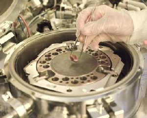
 Graduate student Will Chung displays a hybrid chip being developed in Professor Tomas Palacios' lab. The machine in the background is used to combine the semiconductor materials into one chip.
Photo - Patrick Gillooly
The standard semiconductor material for most of today's computer chips is silicon, and the main way engineers have improved the speed of silicon chips so far is to keep making them smaller. But silicon chips are now approaching their fundamental size limits, says Tomas Palacios, assistant professor in the Department of Electrical Engineering and Computer Science. "We won't be able to continue improving silicon by scaling it down for long," he says. "It's very difficult to make them a lot smaller."
One way around the size limitation is to use new advanced materials for the transistors. "There are several semiconductor materials that offer better performance than silicon," Palacios says. "The problem is, even though they allow for very fast transistors, they cannot compete with silicon in terms of integration and scalability."
A present-day silicon microprocessor chip may contain more than a billion identical transistors, but researchers run into problems when they try to make similar large numbers of transistors using new materials. "They can make one, 10 or even a few hundred that are really fast," Palacios says, but find it very difficult to make them in larger quantities. Companies have spent decades and billions of dollars building up the technology for making silicon chips efficiently and reliably. Given that long and expensive development process, it's hard for any new material to catch up and be competitive, Palacios says.
Two materials, one chip
But it turns out that most of those transistors on a chip — for example, ones used to store information in the chip memory — don't really need to perform at maximum speed. Only a much smaller number, 5 to 10 percent of the total, are actually carrying out the computations and need to be as fast as possible, he says.
The solution that Palacios and his graduate student, Will Chung, developed is one that many other researchers have tried unsuccessfully to achieve: Combining two different kinds of materials on a single, hybrid chip. Conventional silicon would provide the vast majority of the transistors, while a different semiconductor material with better performance would be used for the transistors that need to work faster.
Palacios and Chung created a chip that combines silicon transistors on the same wafer with ones made from gallium nitride, a semiconductor material that has a much better performance than silicon. The results were initially presented in June at the Device Research Conference in Pennsylvania, and are being published in the October issue of the IEEE journal Electron Device Letters.
Instead of trying to grow the high-performance semiconductor material on top of a silicon chip as others have attempted, Palacios and Chung made the new hybrid chip by embedding a gallium nitride layer into the same type of silicon substrate that is used by the silicon electronics industry. This not only produces a faster chip, but one that is highly efficient (having most of the transistors operate at slower speeds means that the chips do not consume too much energy). Moreover, the chips can be manufactured using the standard technology currently used for commercial silicon chips.
Advantages and challenges
Thomas Kazior, technical director of Advanced Microelectronics Technology at Raytheon Integrated Defense Systems, says the new advance addresses some of the present limitations of both silicon and gallium nitride technology. This could "enable a new class of high-performance mixed-signal and digitally controlled RF [radio frequency] circuits for use in a wide range of Department of Defense and commercial applications," he says.
Besides microprocessor chips, the new integrated technology can be used for other applications such as hybrid chips that combine lasers and electronic components on a single chip, and energy-harvesting devices that can harness the pressure and vibrations from the environment to produce enough power to run the silicon components.
Such hybrid chips could also lead to much more efficient cell phone manufacturing, Palacios says. Present-day cell phones generally use at least four or five separate chips made from different semiconductor materials, "With this technology, you could potentially integrate all these functions on a single chip."
Raytheon's Kazior agrees, saying this technology "provides a path to RF 'systems on a chip.'"
At present, the new technique has been used to make chips that are about one square inch in size. Conventional chip manufacturing processes typically use larger wafers, 8 or 12 inches in diameter, so the research now is focused on overcoming the difficulties of scaling up the process to produce these larger chips, without sacrificing quality. "We have several ideas in that direction," Palacios says. "We are already discussing with several companies how to commercialize this technology and fabricate more complex circuits." However, it could take a couple of years to get to the point where it could be commercialized, he says.
Kazior says "To be truly usable this technology needs to be scaled to larger-wafer diameters. In addition, challenges of device reliability and thermal management of the high-power [gallium nitride] transistors need to be addressed."
The research was funded by the DARPA Young Faculty Award, the MARCO Interconnect Focus Center and the MIT Deshpande Center. Device fabrication was carried out at the Microsystems Technology Laboratories and the Nano-Structures Laboratory at MIT.