Jun 1 2010
Recently designed 3-D Hall magnetic-field silicon devices suffer from essential drawbacks. They contain quite many contacts - at least 8 - which complicate the technology realization, impeding the spatial resolution and the necessary miniaturization degree cannot be achieved. A new promising approach and relevant to it 3-D silicon microdevice with four contact only is presented and tested in this paper.
The measurement procedure we have expanded in time and not in space. In this subsequent method is used the same device, i.e. the same transducer region but at a different time. If the interval registration is kept short enough and if the measurement repetition frequency is high enough, the change in the values of components Bx, By and Bz will be negligible.
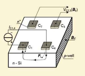
 silicon four-contact Hall device; the measurement principle of Bx-component is shown.
The novel 3-D microsensor consists of a square n-Si structure with four n+-contacts C1, C2, C3 and C4 positioned at the top surface, near to the four corners. A lateral deep p-well ensures the isolation of the active transducer zone by the rest of the substrate.
The operation principle of the new multisensor device is as follows. The in-plane Bx measurement uses a supply current IC1,4. The opposite Lorentz deflections of vertical to the surface components IC1 and - IC4 generate on the contacts C2 and C3 a Hall voltage VC2,3(Bx).
The next measurement step for field By utilizes the current IC1,2, while the Hall voltage is VC3,4(By). The By sensor operation is the same as for Bx. The Lorentz deflections of vertical to the top surface current components - IC1 and IC2 are in opposite directions. Since, on contacts C3 and C4 a Hall voltage VC3,4(By) is generated. The last step realizes the Bz measurement with current IC1,3. The output voltage VC2,4(Bz) is between electrodes C2 and C4.
In this case the horizontal component of IC1,3 is deflected in plane x-y by the Lorentz force FL. Due to the structure symmetry, for a given Bx direction if as a biasing current is used IC2,3 at IC2,3 = IC1,4, the respective magnetic response - VC1,4(Bx) will be equal in value and of opposite sign to the Hall voltage VC2,3(Bx). The offsets VC2,3(0) and VC1,4(0) are almost equal in value and with the same sign since both the identical Hall devices are merged to form subsequently in time a double-Hall sensor for one magnetic-field axis. If as an output signal Vx(Bx) is used the difference Vx(Bx) = VC2,3(Bx) + VC2,3(0) - (-VC1,4(Bx) + VC1,4(0)), the output will be doubled.
The optimised prototypes are realised with silicon planar technology. The dimensions of the active area are 80x80 μm2 have respective channel sensitivities reach Sx = Sy ≈ 27 V/AT and Sz ≈ 36 V/AT. The supply current of the 3-D microsensor is 2mA. The registration of each of the components of the magnetic field Bx, By or Bz is accomplished for a time tone_component ≈ 33.4 μs. The period of total measurement procedure is tfull = 100 μs. This interval is short enough so the changes in Bx, By and Bz values and directions to be losses.
The nonlinearity is no more than NL ≤ 0.2 % at induction B ≤ 0.4 T. The obtained temperature coefficient of magnetosensitivity is low and consist T.C. = 0.1 %/ ºC. The noise power spectral density in the range f ≤ 1 kHz is 1/f type. This noise level for the three channels in our case is lowest in comparison with the known solutions of 3-D silicon Hall microsensors. This is because the sensor contacts are outside the current flow.
The new method and device are patent protection. The practical applicability of this invention includes nanotechnologies, atomic-force microscopy of fluids containing magnetic nano-particles (blood, blood plasma), low-field magnetometry for detecting the variations and perturbations of the earth magnetic field, antiterrorist activities, health etc.
Source: http://www.bas.bg/