Nov 19 2010
Computer chips are the raw material of the Cyber Age. As computer developers come up with machines that process more and more data faster and faster, they push the chip manufacturers closer to the limits of their production technologies.
Researchers at ORNL are developing a method of packing more circuitry into a smaller space on these silicon wafers. Referred to as 100-nanometer lithography, the term reflects the feature resolution required to pack extremely tiny circuits directly onto the microchip wafers. Recent improvements in optical lithography, however, have pushed the requirements for next-generation lithography closer to 70- or 50-nanometer feature size.
The ORNL method may be the technology leap the industry requires for that kind of resolution. Because it uses electron beams to "write" the circuits onto the chips, next-generation lithography is about as fundamentally different from current processes as digital is from analog technology.
"Chip density—transistors per square centimeter—doubles about every two years," says Tommy Thomas, the Instrumentation and Controls Division researcher who is leading the electron-beam lithography project. "The speed of microprocessors doubles about every 18 months. The technology for manufacturing chips to handle that kind of development is becoming strained."
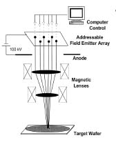
 In the addressable field emitter array concept, electron beams from amorphous diamond cathodes "write" circuit patterns onto a computer chip wafer. The technology could help chip makers attain the degrees of chip density that designers are approaching.
Thomas explains that, to make a chip wafer, manufacturers currently make a chrome-on-glass mask that is four times the size of the chip they want. Lasers are used to illuminate the mask, and the circuit pattern is focused on a photoresist-covered wafer. When light hits it, it releases an electron, and the image is then etched into a circuit.
"The idea comes from photolithography, but as you miniaturize and stack layers, it becomes very complicated," Thomas says. "When you get to a certain point, the lasers can't be focused any smaller."
Thomas and a host of Lab researchers began to ponder new chip-making technologies after David Rasmussen of the Fusion Energy Division, who was on assignment to the SEMATECH consortium, suggested looking into 100-nanometer lithography.
The current state of the art is 200 nanometers. Incidentally, a nanometer is one billionth of a meter.
"We initially considered electron holography, but Edgar Voelkl in the Metals and Ceramics Division suggested simply focusing electrons," Thomas says. "We came up with the idea of programming millions of computer-controlled nano-scale cathodes to emit electrons and using a magnetic lens to focus the electron beams onto a silicon wafer. Each beam spot would fill about 20 to 40 nanometers."
The key to the technology is the amorphous diamond emitter, which is what Thomas calls an electromagnetic cathode coated with amorphous diamond. Amorphous diamond lacks hydrogen, which makes it harder. Multitudes of amorphous diamond emitters would be placed on a chip in what Thomas refers to as the addressable field emitter array, or AFEA. With a successful AFEA process, Thomas says the chip manufacturers could realize incredible yields of chip density.
"The cathodes emit electrons, similar to the way a digital television screen works," Thomas says. "You could fire six million or so programmed emissions at once at a chip. You would need no mask; you would be coding the surface directly with the electrons.
"That's why we say it's like going from an analog to digital technology. In less than one second, you could write a square centimeter with 100-nanometer features. A chip wafer would have 300 one-centimeter squares on it."
Thomas and his colleagues proposed the project three years ago and received DARPA funds to build a prototype, which has resulted in two wafers of 5 × 5-pixel cathode chips.
Larry Baylor of Fusion Energy Division has been measuring current emissions of the AFEAs ("You want current, not voltage, because it's more uniform," Thomas says). The Solid State Division's Doug Lowndes has experimented in making the amorphous diamond by using laser ablation. Thomas counts six ORNL divisions involved in the project—I&C, Fusion Energy, M&C, Solid State, Engineering Technology and Computational Physics and Engineering.
Thomas says the critical issues in the continuing work are whether they can make the amorphous diamond emitters reliable, uniform, stable, controllable and reproducible. "In other words, can we make them do what we need for them to do."
If they can, the limits to the data acrobatics currently performed with microchips will be pushed way beyond what seemed possible just a few years ago. —B.C.
Source: http://www.ornl.gov/