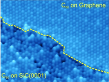
Scientists from the Electronic & Magnetic Materials & Devices (EMMD) Group at the Center for Nanoscale Materials have used cryogenic ultrahigh vacuum scanning tunneling microscopy to observe extremely weak molecule-surface interactions between fullerene C60 deposited over graphene grown epitaxially on silicon carbide substrates.
 STM three-dimensional rendered image of a C60 self-assembled monolayer at a domain boundary of graphene and bare SiC(0001); each C60 molecule is 1 nm in diameter.
The first layer of fullerene C60 molecules assembles itself into well-organized tightly-packed islands. In situ scanning tunneling spectroscopy uncovers a highest occupied molecular orbital–lowest unoccupied molecular orbital gap of 3.5 V, a value close to that of gas and solid-phase C60. This result specifies that there is a smaller quantity of charge transfer between the C60 and the graphene when compared with the adsorption of the C60 onto metallic surfaces.
It is a known fact that interface effects influence the properties of adsorbed molecules. In this case, the organic system has been totally decoupled by the graphene, a perfect two-dimensional material, from the silicon carbide surface reconstruction’s charged interface states. Optimization of biosensors and organic photovoltaics that are based on molecules depends on minimum substrate-molecule interaction in order to maintain intrinsic molecular functionalities. This was realized in this case through an inert graphene ‘barrier’ layer.
EMMD’s objective is to identify, understand, and use constrained geometrical phenomena and novel electron and spin-based materials. Possible advantages include new medical therapies and imaging methods, lowered power dissipation, enhanced data storage efficiency by electrical field-assisted writing and spin current, and improved conversion efficiency in photovoltaic devices.