Nov 19 2012
By fabricating graphene structures atop nanometer-scale "steps" etched into silicon carbide, researchers have for the first time created a substantial electronic bandgap in the material suitable for room-temperature electronics.
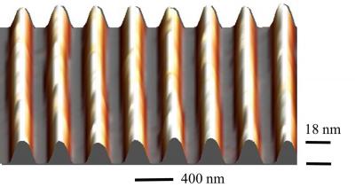
 This is a perspective atomic force microscope (AFM) view of graphitized trenches that are 18 nanometers deep. Credit: Courtesy Georgia Tech
Use of nanoscale topography to control the properties of graphene could facilitate fabrication of transistors and other devices, potentially opening the door for developing all-carbon integrated circuits.
Researchers have measured a bandgap of approximately 0.5 electron-volts in 1.4-nanometer bent sections of graphene nanoribbons. The development could provide new direction to the field of graphene electronics, which has struggled with the challenge of creating bandgap necessary for operation of electronic devices.
"This is a new way of thinking about how to make high-speed graphene electronics," said Edward Conrad, a professor in the School of Physics at the Georgia Institute of Technology. "We can now look seriously at making fast transistors from graphene. And because our process is scalable, if we can make one transistor, we can potentially make millions of them."
The findings were scheduled to be reported November 18 in the journal Nature Physics. The research, done at the Georgia Institute of Technology in Atlanta and at SOLEIL, the French national synchrotron facility, has been supported by the National Science Foundation' Materials Research Science and Engineering Center (MRSEC) at Georgia Tech, the W.M. Keck Foundation and the Partner University Fund from the Embassy of France.
Researchers don't yet understand why graphene nanoribbons become semiconducting as they bend to enter tiny steps – about 20 nanometers deep – that are cut into the silicon carbide wafers. But the researchers believe that strain induced as the carbon lattice bends, along with the confinement of electrons, may be factors creating the bandgap. The nanoribbons are composed of two layers of graphene.
Production of the semiconducting graphene structures begins with the use of e-beams to cut trenches into silicon carbide wafers, which are normally polished to create a flat surface for the growth of epitaxial graphene. Using a high-temperature furnace, tens of thousands of graphene ribbons are then grown across the steps, using photolithography.
During the growth, the sharp edges of "trenches" cut into the silicon carbide become smoother as the material attempts to regain its flat surface. The growth time must therefore be carefully controlled to prevent the narrow silicon carbide features from melting too much.
The graphene fabrication also must be controlled along a specific direction so that the carbon atom lattice grows into the steps along the material's "armchair" direction. "It's like trying to bend a length of chain-link fence," Conrad explained. "It only wants to bend one way."
The new technique permits not only the creation of a bandgap in the material, but potentially also the fabrication of entire integrated circuits from graphene without the need for interfaces that introduce resistance. On either side of the semiconducting section of the graphene, the nanoribbons retain their metallic properties.
"We can make thousands of these trenches, and we can make them anywhere we want on the wafer," said Conrad. "This is more than just semiconducting graphene. The material at the bends is semiconducting, and it's attached to graphene continuously on both sides. It's basically a Shottky barrier junction."
By growing the graphene down one edge of the trench and then up the other side, the researchers could in theory produce two connected Shottky barriers – a fundamental component of semiconductor devices. Conrad and his colleagues are now working to fabricate transistors based on their discovery.
Confirmation of the bandgap came from angle-resolved photoemission spectroscopy measurements made at the Synchrotron CNRS in France. There, the researchers fired powerful photon beams into arrays of the graphene nanoribbons and measured the electrons emitted.
"You can measure the energy of the electrons that come out, and you can measure the direction from which they come out," said Conrad. "From that information, you can work backward to get information about the electronic structure of the nanoribbons."
Theorists had predicted that bending graphene would create a bandgap in the material. But the bandgap measured by the research team was larger than what had been predicted.
Beyond building transistors and other devices, in future work the researchers will attempt to learn more about what creates the bandgap – and how to control it. The property may be controlled by the angle of the bend in the graphene nanoribbon, which can be controlled by altering the depth of the step.
"If you try to lay a carpet over a small imperfection in the floor, the carpet will go over it and you may not even know the imperfection is there," Conrad explained. "But if you go over a step, you can tell. There are probably a range of heights in which we can affect the bend."
He predicts that the discovery will create new activity as other graphene researchers attempt to utilize the results.
"If you can demonstrate a fast device, a lot of people will be interested in this," Conrad said. "If this works on a large scale, it could launch a niche market for high-speed, high-powered electronic devices."