Feb 20 2013
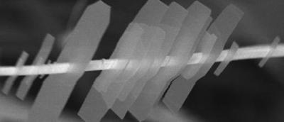
Researchers at North Carolina State University have developed a new type of nanoscale structure that resembles a "nano-shish-kebab," consisting of multiple two-dimensional nanosheets that appear to be impaled upon a one-dimensional nanowire.
 The "shish-kebab " consists of two-dimensional nanosheets strung along a nanowire
But looks can be deceiving, as the nanowire and nanosheets are actually a single, three-dimensional structure consisting of a single, seamless series of germanium sulfide (GeS) crystals. The structure holds promise for use in the creation of new, three-dimensional (3-D) technologies.
The researchers believe this is the first engineered nanomaterial to combine one-dimensional and two-dimensional structures in which all of the components have a shared crystalline structure.
Combining the nanowire and nanosheets into a single "heterostructure" creates a material with both a large surface area and – because GeS is a semiconductor – the ability to transfer electric charges efficiently. The nanosheets provide a very large surface area, and the nanowire acts as a channel that can transmit charges between the nanosheets or from the nanosheets to another surface. This combination of features means it could be used to develop 3-D devices, such as next-generation sensors, photodetectors or solar cells. This 3-D structure could also be useful for developing new energy storage technologies, such as next-generation supercapacitors.
"We think this approach could also be used to create heterostructures like these using other materials whose molecules form similar crystalline layers, such as molybdenum sulfide (MoS2)," says Dr. Linyou Cao, an assistant professor of materials science and engineering at NC State and co-author of a paper on the research. "And, while germanium sulfide has excellent photonic properties, MoS2 holds more promise for electronic applications."
The process, Cao says, is also attractive because "it is inexpensive and could be scaled up for industrial processes."
To create the nano-shish-kebabs, the researchers begin by creating a GeS nanowire approximately 100 nanometers in width. The nanowire is then exposed to air, creating nucleation sites on the wire surface through weak oxidation. The nanowire is then exposed to GeS vapor, which forms into two-dimensional nanosheets at each of the nucleation sites.
"Our next step is to see if we can create these heterostructures in other materials, such as MoS2," Cao says. "We think we can, but we need to prove it."