Jan 31 2014
Since continuous miniaturization in microelectronics is already starting to reach the physical limits, researchers are seeking new methods for device fabrication. One promising candidate is the DNA origami technique in which individual strands of the biomolecule self-assemble into arbitrarily shaped nanostructures.
The formation of entire circuits, however, requires the controlled positioning of these DNA structures on a surface – something which previously has only been possible using very elaborate techniques. Now, researchers at the Helmholtz-Zentrum Dresden-Rossendorf (HZDR) have come up with a simpler strategy which combines DNA origami with self-organized pattern formation. The researchers' method is featured in the scientific journal Nanoscale's current issue (DOI: 10.1039/C3NR04627C).
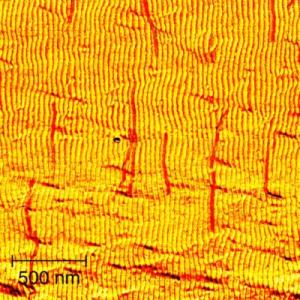
 What looks like sand dunes is actually smaller than a single grain of sand. Thanks to electrostatic surface interactions, DNA nanotubes (shown here in red) align along the prefabricated nanopattern on a silicon surface.Credit: Helmholtz-Zentrum Dresden-Rossendorf
Dr. Adrian Keller of the HZDR Institute of Ion Beam Physics and Materials Research describes the new method: "Its beauty lies with the fact that we're allowing nature to simply run its course as soon as we've created the necessary framework." In the DNA origami technique, the DNA structures self-assemble as long strands of the biomolecule fold into complex, predefined nanoscale shapes by pairing with multiple smaller DNA strands. The physicists used the technique to produce small tubes with lengths of 412 nanometers and diameters of six nanometers. These structures can be used as scaffolds for manufacturing nanoelectronic components like nanowires.
In order to align these nanotubes on the surface, the researchers drew on a principle of self-organization that is actually quite common in nature. Wind may for instance form ordered patterns on a sandy beach. "Similar processes are at work here," explains Keller. "We irradiate the surface onto which we want to place the nanostructures - in our case, the silicon wafers - with ions. This results in the spontaneous appearance of ordered nanopatterns resembling miniature sand dunes. At that point, our job is pretty much done as natural processes are taking over and doing all the work."
Through electrostatic interactions between the charged DNA nanostructures and the charged surface, the nanotubes align themselves in the valleys of the dunes. Says Keller: "This technique works so well that not only do the small tubes follow the wavy patterns, they even replicate occasional pattern defects. Meaning this technique should also allow for production of curved nanocomponents." The maximum degree of alignment the Dresden researchers were able to obtain was at a pattern wavelength of 30 nanometers. "True, we're only looking at a total yield of 70 percent of nanotubes that perfectly follow the pattern," concedes Keller. "But it's still impressive considering the natural process we used."
Because unlike previous approaches, according to Keller, the new technique is quick, cheap, and simple. "Until now, we had to draw on lithographic techniques plus treat the surface with chemicals in order to align the DNA nanostructures. Although this does produce the desired outcome, it nonetheless complicates the processes. Our new technique offers a much simpler alternative." Since aligning the small tubes is based exclusively on electrostatic interaction with the prestructured surface, using this particular method the nanotubes could also be arranged into more complex arrays such as electronic circuits. Keller is convinced that they can be attached to individual transistors, for instance, and connect them electrically: "This way, DNA based nanocomponents could be integrated into technological devices and contribute to further miniaturization."