Jun 23 2014
Staff and students at schools and universities throughout Denmark are excited about a new facility housing multiple scanning electron microscopes that has opened within Nanoteket, a nanotechnology teaching laboratory at the Technical University of Denmark (DTU), near Copenhagen. The laboratory operates in collaboration with the university’s physics department and centre for electron nanoscopy. The latest project has been funded by three private foundations - Villum Fonden (the main sponsor), Otto Mønsteds Fond, and Marie & M. B. Richters Fond.
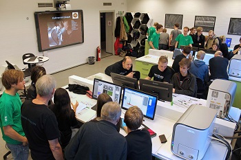
 The new SEM laboratory within Nanoteket at the Technical University of Denmark is populated with five JEOL NeoScopes from Nikon Metrology.
To supplement the university’s existing scanning tunnel microscopes and atomic force microscopes dedicated to teaching, five scanning electron microscopes were purchased from Nikon Metrology in February 2014 as the basis for the new facility. They are being used by students and undergraduates from all over Denmark to carry out physics experiments that were previously impossible within the country’s academic structure, as there was no SEM teaching laboratory available for high school students to use.
Researchers and students alike, in particular those from secondary schools, have shown great interest in the microscopes, with 130 visiting in the first month alone. Nanoteket attracts around 3,500 visitors per year, including 1,600 school pupils. Staff expect that the scanning electron microscopes will attract an additional 500 or so interested people.
Nanoteket is managed by Ole Trinhammer, the head of the laboratory, and Louise Haaning, project manager responsible for the electron microscopes. She holds an MSc in Engineering from DTU within the field of physics and nanotechnology and until 2011 worked as a teaching assistant at Nanoteket. Eleven physics and nanotechnology students from DTU are currently employed as teaching assistants, so it is primarily young people who teach other young people.
The considerable benefit of this approach is perfectly summarised by Irvin Svensson, a teacher at Rosborg High School in Vejle, Jutland, who usually accompanies a class of students to DTU once a year. He said, “It’s always a delight to visit the university and the arrival of the new SEM equipment in the physics department is incredible.
“Our students enjoy the microscopy exercises, as it’s a lot of fun to peer into a microscope and enter a whole new world.
“The students from DTU, rather than the staff, help and coach visitors from schools and it’s fantastic to see how they deal with them. It’s much more exciting for pupils to work with someone who’s only a bit older than they are.”
Louise Haaning added, “We need the scanning electron microscopes for educational purposes, as we want to teach students from schools and universities about nanotechnology and electron microscopy and give them hands-on experience with such equipment.”
An advantage of the JEOL NeoScope SEM from Nikon Metrology is that it has both a secondary electron detector and a back-scattered electron detector.
Most SEMs have secondary electron imaging to produce very high-resolution images of a sample surface with a large depth of field, revealing 3D detail down to single figure nanometres.
However, the NeoScope’s ability to detect electrons that are back-scattered from the sample means that the instrument can also detect the amount and distribution of different elements within the specimen. Thus the microscope can provide much more information and broadens the range of possible applications.