Nov 24 2014
U.S. Naval Research Laboratory (NRL) scientists, in collaboration with researchers from the University of Manchester, U.K.; Imperial College, London; University of California San Diego; and the National Institute of Material Science (NIMS), Japan, have demonstrated that confined surface phonon polaritons within hexagonal boron nitride (hBN) exhibit unique metamaterial properties that enable novel nanoscale optical devices for use in optical communications, super-resolution imaging and improved infrared cameras and detectors.
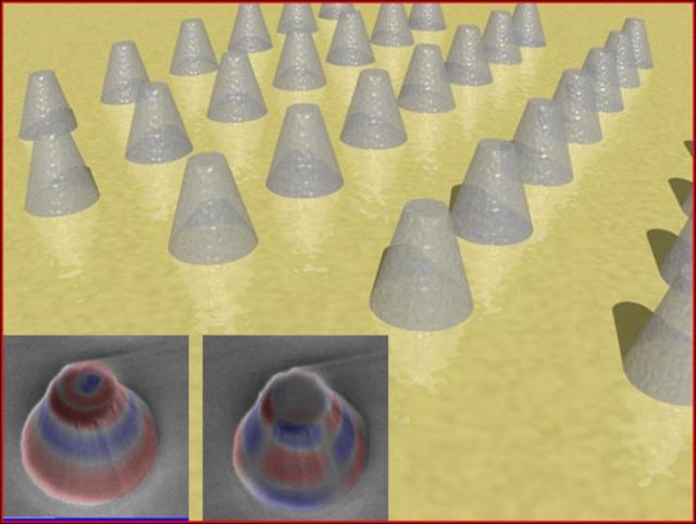
 Periodic arrays of cone-shaped hexagonal boron nitride nanoantennas, depicted magnified image above, were used to confine hyperbolic polaritons in all three dimensions. This enabled the researchers to fundamentally probe the novel optical properties within these materials and demonstrate the highly directional, low loss hyperbolic polaritons that are confined within the volume of the antennas. These results provide the first foray into natural hyperbolic materials as building blocks for nanophotonic devices in the mid-infrared to terahertz spectral range. Credit: U.S. Naval Research Laboratory
Metamaterials are artificial composites of various materials designed to exhibit optical properties not anticipated in nature. One such property is hyperbolicity, whereby a material exhibits both metallic- and dielectric-like optical responses simultaneously along different crystal axes. These hyperbolic metamaterials are the basis for many potential applications such as 'hyperlenses,' used for imaging of nanoscale objects not observable using conventional optics.
"Our examination into the characteristics of hBN reveal the first experimental observation of sub-diffractional guided waves confined in all three dimensions, using a natural hyperbolic material," said Joshua Caldwell, Ph.D., Electronics Science and Technology Division, Power Electronics Branch. "This may, in turn, lead to the development of disruptive technologies such as the nanoscale equivalent of an optical fiber due to the volume-bound confinement of sub-diffractional modes within hBN."
Optic phonons, or crystal vibrations that can be excited with infrared light, can also be used to confine light to dimensions much smaller than the wavelength of light, while maintaining record-high efficiencies. These surface phonon polaritons are analogous to electron oscillations in metals or doped-semiconductors, called plasmons, but offer the benefit of low losses and operation in the infrared to terahertz spectral regions.
As a van der Waels crystal -- a layered crystal structure similar to graphene or graphite -- hBN was demonstrated to be two orders of magnitude more efficient than hyperbolic metamaterials shown to date, says Caldwell. Unlike metallic/dielectric hyperbolic metamaterials, hBN also provides the additional functionality of both types of hyperbolicity, allowing both the in-plane and out-of-plane crystal axes to behave metallic- (reflective) or dielectric-like (transparent) simply by changing the wavelength of the exciting light. This mixing of both types of hyperbolic behavior is to this point unique and allowed the fundamental comparison of antennas within these two regimes.
Using the natural hyperbolic behavior of hBN, the researchers were able to demonstrate that light could also be confined within optical antennas -- up to 86 times smaller than the wavelength of light, for instance confinement of 6.8 micrometers of light into a 0.08 micrometer tall antenna -- while maintaining record-high efficiencies due to the low-loss nature of the dielectric crystal.
The researchers were able to further demonstrate that the resonance wavelength of the hyperbolic polaritons confined within these antennae was dependent only upon the aspect ratio (height/diameter), and was nominally independent upon the actual size and/or shape -- demonstrating that antennas could be defined for a given application simply by controlling this ratio, thereby making them compatible to a wide array of device form-factors. This could enable frequency selective operation and nanophotonic circuits, as well as provide an operational material for mid-infrared imaging of nanoscale objects.
The research team also demonstrated that the resonance response exhibited not a single mode, but four separate series, and according to Caldwell, a change in the wavelength and/or the angle of the incoming light with respect to the sample surface could isolate each series, providing the first complete description of these novel, three-dimensionally confined hyperbolic polariton modes.
Further discoveries found these breakthroughs could have an impact in areas such as enhanced infrared or molecular spectroscopy, improved functionality for nanophotonic circuits and devices for use in infrared cameras, detectors and weapons guidance systems, and tailored thermal emission sources.