Aug 10 2016
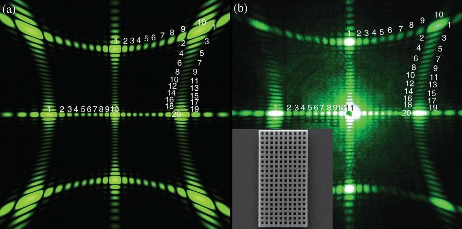
 EXPERIMENTALLY OBTAINED AND SIMULATED DIFFRACTION PATTERNS FOR A SAMPLE. CREDIT: ITMO UNIVERSITY
Scientists from Australia and Russia have discovered a new method for counting microscopic particles in optical materials with the help of a laser.
A light beam traveling through this material splits and develops a characteristic pattern comprising of several bright spots on a projection screen. The researchers discovered that the number of these spots correlates exactly to the number of scattering microscopic particles present in the optical material.
It is possible to determine the shape and structure of an optical material without using atomic-force or electron microscopy that is expensive. The new method will indeed play a major role in designing optical devices in a rapid manner. This research was featured in Scientific Reports.
Optical circuits can be developed using devices that are capable of amplifying optical signals, bringing them into focus, and then rotating and modifying their type of motion. Scientists are currently using artificial optical materials, such as metamaterials and photonic crystals, as ordinary lenses are not capable of handling these tasks at nanoscale.
These artificial optical materials can monitor the propagation of light in a number of extraordinary ways. Fabricating optical materials with the required properties is a difficult process that requires constant enhancement.
A team of researchers from ITMO University, Ioffe Institute, and Australian National University have for the very first time suggested the usage of an optical diffraction method for examining the structure of photonic crystals. In this method, the generated light pattern is considered and the sample is exposed to a laser beam.
The study revealed that the number of these spots is equivalent to the number of scattering microscopic particles present in the sample structure. Earlier, it was possible to see and count these small particles only with the help of costly and powerful atomic-force or electron microscopes.
The light senses heterogeneity. Depending on the shape and relative position of the scatterers, the light wave continues to propagate differently behind the sample. In other words, the structure of the sample affects the diffraction pattern, which will be projected on the screen. We found out that looking at the pattern, it is possible to determine the precise number of scatterers in the material. This helps understand not only the type of the sample lattice (square, triangular), but also to establish its structure (20 to 20 particles, or 30 to 15) just by counting light spots on the screen.
Mikhail Rybin, Senior Researcher, ITMO University
This new method is considered to be an affordable alternative to the costly atomic-force or electron microscopy and in this situation it does not destroy the sample. “Even a schoolboy can buy a laser pointer, adapt a small lens to focus the light better, fix the sample and shine a laser beam on it,” notes Mikhail Rybin. “In addition, our method makes it possible to study optical materials without changing their structure in contrast to electron microscopy, where the sample surface has to be covered with conductive metal layer, which impairs optical properties of the sample.”
Scientists have previously used this new method to examine the shift between two main types of optical materials, metasurfaces and photonic crystals. In this research, the researchers established the lattice parameters, which decide the possibility of the light perceiving the material as a two-dimensional photonic crystal or a metasurface.
The scattering particles, in both the types of optical materials, are positioned in a flat lattice. These scattering particles include balls, rings, and cylinders of 200-300 nanometers. The light identifies the sample as a set of individual particles in the case of two-dimensional photonic crystal.
By traveling through it the light produces a fancy pattern on the screen just behind the sample. Only one bright spot is highlighted on the screen and this indicates that the scattering particles are placed next to each other such that they are not seen by the light as separate particles. The light thus travels through the sample without splitting.
The distance between the particles should be smaller than the wavelength of light in order to allow the light beam to travel through a metasurface. Based on calculations, some structures will need a lattice where the distance between particles is 2 to 3 times smaller than the wavelength of light. However, the meta-properties often manifest themselves at greater distances between the particles. It is also important to identify the maximum allowable distance, as decreasing the structure by a single nanometer makes the technology a lot expensive.
For example, it turned out that for the light comprising a wavelength of 530 nanometers (green color), the distance of 500 nanometers between the scattering particles is already sufficient.
A green light beam perceives the structure with a period of 500 nanometers as a homogenous material. Therefore, sometimes it is not necessary to fabricate a lattice with a period much smaller than the wavelength of light. And producing larger structures is much easier from technological standpoint. For one wavelength, the material will act as a photonic crystal and as a metasurface for another. That is why designing such structures, we can evaluate maximum lattice period with laser.
Mikhail Rybin, Senior Researcher, ITMO University