Jul 25 2017
An international team, for the very first time, realized direct writing of silver nanostructures by using an electron beam applied to a substrate. Silver nanostructures are capable of concentrating visible light at the nanoscale. Promising applications include sensor design for detecting extremely minute traces of particular molecules and also devices for optical information processing.
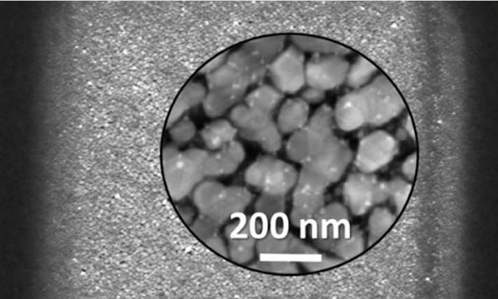
 Scanning electron micrographs show a 10-micron planar deposition. The constituting silver crystals are about 100 nanometres in size. Credit: HZB/ ACS Applied Materials &Interfaces (2017)
A scanning electron microscope (SEM) is unrivaled when it comes to extremely fine, precise features. Complex features can be directly deposited onto a substrate in a single step (Electron-Beam-Induced Deposition (EBID)) by a focused electron beam. While this is a proven technique for copper, platinum, gold and further metals, direct electron beam writing of silver continued to be elusive. However, the noble metal silver provides particularly interesting and promising applications in nano-optics in information technology. The local deposition of silver nanocrystals by EBID has been successfully realized for the very first time by a team from the HZB and the Swiss Federal Laboratories for Materials Science and Technology (EMPA). The results have been recently published in the journal of the American Chemical Society's ACS Applied Materials Interfaces.
Challenging chemistry
The chemistry of typical silver compounds is considered to be extremely challenging. They are highly reactive and difficult to evaporate. They tend to chemically react with the reservoir walls during the heating in the injection unit. Along their route from the reservoir to the tip of the needle, these compounds freeze all over again when the temperature drops even slightly, thus obstructing the tube.
It took us a lot of time and effort to design a new injection unit and find a suitable silver compound. Finally, we managed it. The compound silver dimethylbutyrate remains stable and dissociates only in the focus of the electron beam.
Dr. Katja Höflich, HZB Physicist, who performed the experiments as part of a Helmholtz Postdoctoral Fellowship at EMPA
The EBID method was used by Höflich and her colleagues to develop sharply defined areas of small silver nanocrystals for the first time.
Writing with the electron beam
The principle works in the following manner: small amounts of a precursor substance – usually a metal-organic compound – are inserted into the vacuum chamber of the SEM close to the surface of the sample by using a needle. The electron beam falling on the sample surface results in the precursor molecules getting dissociated, following which their non-volatile constituents are deposited in place. The electron beam is capable of moving like a pen over the substrate in order to produce the preferred features. This works even in three dimensions for a number of precursor substances.
Silver is a light concentrator
The fabricated silver nanostructures comprise of incredible optical properties: visible light is capable of exciting the free electrons in the metal into oscillations known as plasmons. These plasmons are escorted by an extreme lighting. The color and intensity of this scattered light provide information about the composition of the surfaces. This effect can be employed in Raman spectroscopy in order to detect the fingerprint of particular molecules that bind to the silver surface – down to the level of an independent molecule. Silver nanostructures are thus considered to be good candidates as sensors for explosives or various other hazardous compounds.
A vision for the future: components for optical computing
It is possible to have additional applications in future information technology: complex silver nanostructures could comprise of the foundation for purely optical information processing. This was realized by refining the process, resulting in the possibility of directly writing complex features as was earlier done for several other precursor compounds.