Nov 13 2017
2D-materials are made up of special lattice structures. In general, atoms in the same layer are bound by the covalent bond, while the force present between layers is van der Waals coupling. These materials comprise of super clean surfaces without any dangling bonds.
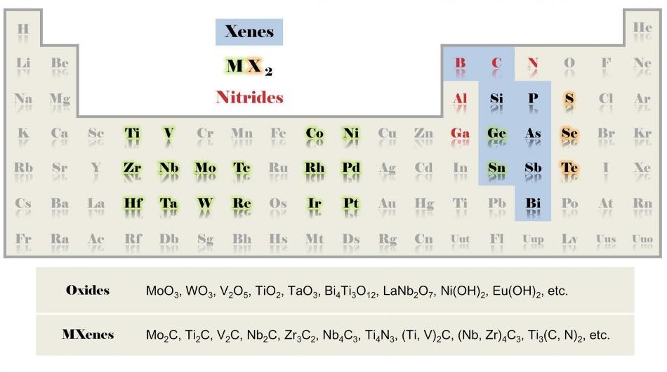
 This figure shows the distribution of elements of different 2-D materials. CREDIT ©Science China Press
The design of heterojunctions will be flexible when 2D-materials are employed to constitute heterojunctions. The heterojunctions developed by a wide range of 2D-materials have beneficial properties compared with their equivalent single-component 2D-material, such as optimizing band alignment, charge transfer, bandgap and optical properties. The research of heterojunctions is considered to be a popular topic in 2D-material field.
A review "Chemical vapor deposition growth of two-dimensional heterojunctions" by Prof. Zhongming Wei at Institute of Semiconductors, Chinese Academy of Sciences, has been recently published in SCIENCE CHINA Physics, Mechanics & Astronomy. In this review, the methods of chemical vapor deposition (CVD) for fabricating 2D heterojunctions are mentioned based on research performed over the last few years. The development history of heterojunctions of 2D-materials is initially introduced. This is followed a discussion on the influences of varied growth conditions on heterojunctions. Finally, a few other methods for preparing heterojunctions are referred.
The transfer method is considered to be a good technique for heterojunctions of 2D-materials in labs. Researchers can use this simple method in order obtain the exact heterojunction they want. However, it is not enough for a range of applications, a stable and efficient technique is essential. The chemical vapor deposition is introduced a posible mehtod to create heterojunctions. The chemical vapor deposition method is sensitive to the variations of growth conditions. It is a vital research topic to determine influences of varied factors on the growth process and final heterojunctions. This review categorizes the factors into temperature, precursor, lattice mismatch, substrate, carrier gas composition, and carrier gas flow rate. The obtained heterojunctions will have different components or structures when one of the factors changes. These factors also influence each other. Hence, the anticipated heterojunctions of 2D-materials cannot be be fabricated by only altering one parameter of the chemical vapor deposition system. For instance, when different precursors are employed, it is essential to reset the growth temperature due to the varying evaporating temperatures of different precursors. Besides these, the method via sulfuring patterned films, such as oxide films, metal films and other component films, to fabricate heterojunctions is also reffered to.
More research is essential for solving problems in the fabrication of heterojunctions of 2D-materials. MOCVD and MBE can also be considered as possible options of the fabrication technique.