Sep 25 2018
Researchers who develop optoelectronics — electronic devices with the ability to interact with light to carry out tasks — are highly intrigued by the potential of semiconducting or metallic materials to absorb, reflect, and act upon light. At present, researchers from the Rice University have devised a technique for finding out the properties of atom-thin materials that seem propitious in refining the modulation and manipulation of light.
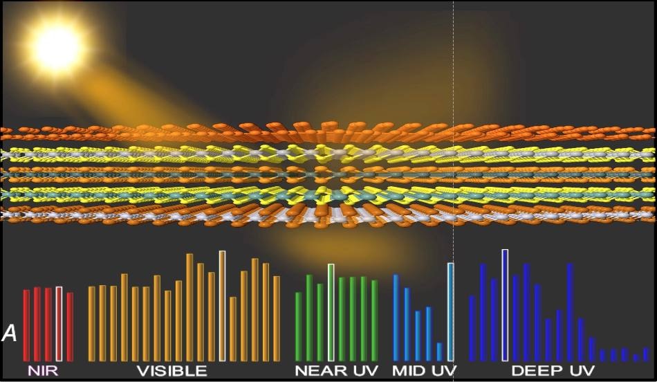
 Rice researchers modeled two-dimensional materials to quantify how they react to light. They calculated how the atom-thick materials in single or stacked layers would transmit, absorb and reflect light. The graphs above measure the maximum absorbance of several of the 55 materials tested. (Image credit: Yakobson Research Group)
Since the time when graphene, a flat lattice of carbon atoms, was invented in 2001, two-dimensional (2D) materials have been a hot topic of research. From that time, researchers have raced to create, in theory or in the lab, innovative 2D materials with different electronic, optical, and physical properties.
To date, a comprehensive guide elaborating on the optical properties exhibited by such materials as ultrathin transmitters, reflectors, or absorbers is not available.
The Rice lab of materials theorist Boris Yakobson took this up as a challenge. Yakobson and his colleagues, graduate student and lead author Sunny Gupta, postdoctoral researcher Sharmila Shirodkar, and research scientist Alex Kutana, used sophisticated theoretical techniques for computing the maximum optical properties of 55 2D materials.
The important thing now that we understand the protocol is that we can use it to analyze any 2D material. This is a big computational effort, but now it’s possible to evaluate any material at a deeper quantitative level.
Sunny Gupta, Lead Author
The study, which will be published this month in the American Chemical Society journal ACS Nano, describes the monolayers’ transmittance, absorbance, and reflectance properties, collectively known as TAR. At the nano-level, light has the ability to interact with materials in distinctive ways, initiating electron-photon interactions or activating plasmons that absorb light at one frequency and emit it in a different frequency.
The ability to manipulate 2D materials allows scientists to design ever smaller devices such as light-driven circuits or sensors. However, primarily, it assists in learning the extent of sensitivity of a material to a specific wavelength of light, from infrared to visible colors to ultraviolet.
Generally, the common wisdom is that 2D materials are so thin that they should appear to be essentially transparent, with negligible reflection and absorption. Surprisingly, we found that each material has an expressive optical signature, with a large portion of light of a particular color (wavelength) being absorbed or reflected.
Boris Yakobson, Theorist
The colleagues expect polarizing filters and photodetecting and modulating devices to be feasible applications for 2D materials with directionally dependent optical properties. “Multilayer coatings could provide good protection from radiation or light, like from lasers,” stated Shirodkar. “In the latter case, heterostructured (multilayered) films—coatings of complementary materials—may be needed. Greater intensities of light could produce nonlinear effects, and accounting for those will certainly require further research.”
The scientists modeled 2D stacks and also single layers. “Stacks can broaden the spectral range or bring about new functionality, like polarizers,” stated Kutana. “We can think about using stacked heterostructure patterns to store information or even for cryptography.”
In the outcomes, the scientists verified that stacks of graphene and borophene are extremely reflective of mid-infrared light. The most striking finding was that a material composed of over 100 single-atom layers of boron — which would still be only around 40 nm thick — would reflect more than 99% of light from the infrared to ultraviolet, surpassing the performance of bulk silver and doped graphene.
There is an added advantage that goes well with Yakobson’s artistic sensibility as well. “Now that we know the optical properties of all these materials—the colors they reflect and transmit when hit with light—we can think about making Tiffany-style stained-glass windows on the nanoscale,” he said. “That would be fantastic!”
The U.S. Army Research Office and the Robert Welch Foundation supported this study. Computing resources were provided by the National Science Foundation-supported DAVinCI cluster at Rice, administered by the Center for Research Computing and procured in partnership with Rice’s Ken Kennedy Institute for Information Technology, the Department of Defense High Performance Computing Modernization Program, and the Department of Energy Office of Science’s National Energy Research Scientific Computing Center.