Feb 21 2019
A new method has been developed by EPFL researchers to regulate and standardize the growth of nanowires on silicon surfaces.
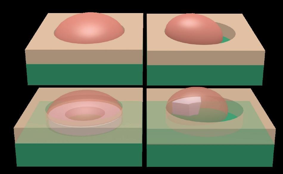
 Two different configurations of the droplet within the opening – hole fully filled and partially filled and bellow illustration of GaAs crystals forming a full ring or a step underneath the large and small gallium droplets. (Image credit: Jamani Caillet/EPFL)
This latest breakthrough could present new opportunities for growing nanowires on electronic platforms, with promising applications such as better energy conversion in solar panels and the incorporation of nanolasers within electronic chips.
Nanowires measure just 5–100 nm in diameter (a nanometer is a millionth of a millimeter) and have the ability to transform the technology around people. These small and needle-shaped crystalline structures can change the way light or electricity travels through them.
Nanowires are capable of emitting, concentrating, and absorbing light, and hence, they may be used for adding optical functionalities to electronic chips. For instance, with the help of these structures, lasers can be directly generated on silicon chips and single-photon emitters can be integrated for coding purposes. In addition, nanowires could even be used in solar panels to enhance the way sunlight is changed into electrical energy.
To date, it has not been possible to recreate the process of developing nanowires on silicon semiconductors. In fact, no method was available to constantly create uniform nanowires in particular positions. However, the research team from EPFL’s Laboratory of Semiconductor Materials managed by Anna Fontcuberta i Morral, along with colleagues from the IOFFE Institute and MIT, has developed a new way to grow nanowire networks in a fully reproducible and highly controlled way. It is important to infer what exactly occurs during the growth of nanowires, which goes against the presently accepted concepts. The results of the study have been reported in Nature Communications.
We think that this discovery will make it possible to realistically integrate a series of nanowires on silicon substrates. Up to now, these nanowires had to be grown individually, and the process couldn't be reproduced.
Fontcuberta i Morral, Associate Professor, Laboratory of Semiconductor Materials, EPFL
Getting the right ratio
In the regular process used for developing nanowires, extremely small holes are made in silicon monoxide and these are subsequently filled with a nanodrop of liquid gallium. When this substance comes into contact with arsenic, it solidifies. However, this process causes the substance to become hard at the nanoholes’ corners, which implies that it is not possible to predict the angle at which the nanowires will grow. Researchers were looking for a method to develop uniform nanowires and regulate their position.
Studies aimed at regulating the production process have always concentrated on the hole’s diameter; however, this method did not prove to be effective. Now, the EPFL team has demonstrated that the growth of nanowires can be perfectly controlled by modifying the hole’s diameter-to-height ratio. The substance at the right ratio will harden in a ring around the edge of the hole, which inhibits the nanowires from forming at a non-perpendicular angle. The process developed by the research team should work for all different kinds of nanowires.
It’s kind of like growing a plant. They need water and sunlight, but you have to get the quantities right.
Fontcuberta i Morral, Associate Professor, Laboratory of Semiconductor Materials, EPFL
This latest production method will be highly significant for nanowire research, and more samples should be developed shortly.