Jun 27 2019
Apart from speeding up computers, nanowires have the potential to make solar cells more efficient and LEDs more colorful. That is, if the extremely small semiconductors are able to transform electric energy into light energy, and vice versa, at the correct wavelengths.
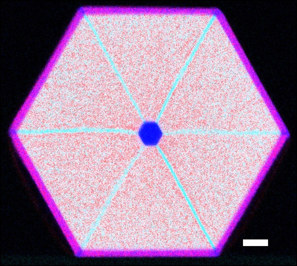
 Cross-section of a nanowire featuring a gallium arsenide core, an indium aluminum arsenide shell, and an indium gallium arsenide capping layer (gallium is shaded blue, indium red and aluminum cyan). For comparison, the white bar indicates a scale of 30 nanometers. The image was produced by energy-dispersive X-ray spectroscopy. (Image credit: HZDR/René Hübner)
Researchers at Helmholtz-Zentrum Dresden-Rossendorf (HZDR) have now successfully created nanowires equipped with operating wavelengths. These wavelengths can be easily chosen across a broad range–by merely modifying the structure of the shell.
Nanowires that are finely tuned could take on many roles in an optoelectronic component, without the necessity to resort to an assorted number of materials. As the researchers have reported in Nature Communications, that would render the components more cost-effective, robust and easier to integrate.
Nanowires are known to be highly versatile. The microscopic elements can be utilized for miniaturized electronic and photonic components in nanotechnology. Solar cells, optical circuits on chips, innovative quantum technologies LEDs, and novel sensors are the applications of nanowires. Free-standing nanowires guarantee the adaptability of the latest semiconductor technologies with traditional silicon-based technologies. Since there is minimal contact with the silicon substrate, nanowires overcome the usual challenges faced when integrating varied materials.
For their analysis, which lasted a number of years, the Dresden team initially set about developing nanowires from gallium arsenide—semiconductor material—on silicon substrates. In the subsequent step, the wafer-thin wires were enclosed in another layer of material to which the researchers added indium as an extra element. Their objective: the materials’ mismatched crystal structure was meant to promote a mechanical strain in the wire core, which alters the electronic characteristics of the semiconductor material, that is, gallium arsenide.
For example, the semiconductor bandgap becomes tinier, causing the electrons to become more mobile. To amplify this effect, the researchers continued to add more amounts of indium to the shell, or increased the thickness of the shell. The outcome went much beyond the expectations.
Taking a known effect to extremes
What we did was take a known effect to extremes. The seven percent of strain achieved was tremendous.
Dr Emmanouil Dimakis, Study Lead, Helmholtz-Zentrum Dresden-Rossendorf
The study involved scientists from TU Dresden, HZDR, and DESY in Hamburg.
At this degree of strain, Dimakis had anticipated seeing disorders taking place in the semiconductor materials—in their experience, the wire core either bends or defects emerge.
According to the researchers, the reason for the absence of such disorders can be attributed to the unique experimental commotions. The researchers initially grew very thin gallium arsenide wires, which were about five thousand times finer than a human hair. Next, they managed to create the wire shell at extraordinarily low temperatures. By then, surface diffusion of atoms is more or less frozen, causing the shell to grow uniformly around the wire core.
The scientists reinforced their finding by performing a number of separate series of measurements at Dresden facilities, and also at the high-brilliance X-ray light sources Diamond in England and PETRA III in Hamburg.
The remarkable outcomes pushed the team to undertake more investigations: “We shifted our focus to the question of what triggers the extremely high strain in the nanowire core, and how this can be used for certain applications,” Dimakis recollected. “Scientists have been aware of gallium arsenide as a material for years, but nanowires are special. A material may exhibit completely new properties at the nanoscale.”
Potential applications for fiber-optic networks
The scientists realized that it is the high strain that allowed them to move the bandgap of the gallium arsenide semiconductor to extremely low energies, making it adaptable even for fiber-optic network wavelengths, which is indeed a technological milestone. Earlier, this spectral range could only be realized through unique alloys consisting of indium, which resulted in several technological issues owing to the material mix.
Nanowires can be produced using high-precision techniques. For this purpose, a unique system was installed at HZDR’s molecular beam epitaxy laboratory, about four years ago. The self-catalyzed growth of nanowires from beams of molecules or atoms is attained in the laboratory; in ultra-high-vacuum, the beams are focused onto silicon substrates.
Emmanouil Dimakis contributed immensely in setting up the laboratory. A large part of the studies reported in the present publication were performed by Leila Balaghi as part of her doctorate.