Oct 6 2020
According to predictions from a new study performed by an international group of researchers, diamond can conduct electricity similar to metals when it is deformed to nanoscale strains.
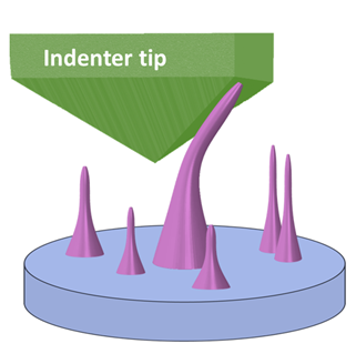
 The scientists applied pressure on the diamond nano-needles by pushing a probe onto the nano-needles. Image Credit: Massachusetts Institute of Technology (MIT).
The team was headed by Nanyang Technological University, Singapore (NTU Singapore) and the Massachusetts Institute of Technology (MIT), United States.
The research team, which also included investigators from the Skolkovo Institute of Science and Technology (Skoltech) in Russia, used computer simulations to demonstrate early proof of concept.
According to this concept, when mechanical strain is applied to nanoscale diamond needles, it may reversibly change their geometry and thus their electrical characteristics, imparting them a metal-like conductivity at ambient pressure and temperature.
Published in the Proceedings of the National Academy of Sciences of the United States of America on October 5th, 2020, the new study may lead to upcoming applications in power electronics that are employed in a wide range of machines, from electrical appliances and cars to smart grids, optical devices, highly efficient light-emitting diodes (LEDs), and quantum sensing, which improves and enhances what sensors can presently do.
The study’s corresponding authors are NTU President and Professor Subra Suresh, MIT Professor Ju Li, and MIT Principal Research Scientist Ming Dao. The authors’ list includes Zhe Shi, a graduate student from MIT, and Evgenii Tsymbalov and Professor Alexander Shapeev from Skoltech.
The study results follow an experimental finding made by an NTU-Hong Kong-MIT research team headed by Professor Suresh, who reported in a 2018 article published in the Science journal that diamond nano-needles—each measuring around a thousand times thinner than a single strand of human hair—can be stretched and bent significantly so that they revert back without being impaired upon releasing the strain.
The extraordinarily high hardness and stiffness of the diamond combined with its number of extreme physical characteristics make it a preferred candidate material for many different applications.
The latest discovery also provides new opportunities for innovative use of diamonds in the fields of power electronics, quantum information, and photonics, including the design of highly efficient photodetectors, emitters, and quantum sensors, and also in biomedical imaging applications.
The ability to engineer and design electrical conductivity in diamond without changing its chemical composition and stability offers unprecedented flexibility to custom-design its functions. The methods demonstrated in this work could be applied to a broad range of other semi-conductor materials of technological interest in mechanical, microelectronics, biomedical, energy and photonics applications, through strain engineering.
Subra Suresh, Distinguished Professor and President, Nanyang Technological University, Singapore
From Insulator to Metal-Like Conductor
Materials that allow an electric current to easily pass through are called electrical conductors, whereas materials, like diamond, that do not, are known as electrical insulators.
Diamonds that exist in a majority of forms are good electrical insulators and this can be attributed to their ultra-wide bandgap of 5.6 electron volts (eV). In other words, a huge amount of energy is required to activate the electrons in the material before they can behave as carriers in an electric current. A smaller bandgap makes it relatively easier for current to flow.
With the help of computer simulations that involved analyses of mechanical deformation, quantum mechanics, and machine learning, the researchers learned that this bandgap can be narrowed by elastically deforming the diamond nano-needle. They achieved this by bending it as a diamond probe pushed it from the side, as shown in the above image.
The team demonstrated that when the amount of strain on the diamond nano-needle is increased, its estimated bandgap narrowed—which indicated greater electrical conductivity. They also noted that this bandgap entirely vanished near the highest amount of strain that could be tolerated by the needle before breaking down.
The researchers also demonstrated that this metallization of diamond at the nanometer scale can possibly be realized without activating phase transformation or phonon instability from diamond to graphite—the soft material used in pencils.
To train machine learning algorithms, the team subsequently applied the simulation results to detect general conditions for acquiring optimal electrical conductivity of nano-scale diamond in numerous geometrical configurations.
While the scientific study is still at the early stage, it definitely offers opportunities for additional development of promising devices that have unparalleled characteristics and performance.
We found that it’s possible to reduce the bandgap from 5.6 eV all the way to zero. The point of this is that if you can change continuously from 5.6 to zero eV, then you cover all the range of bandgaps. Through strain engineering, you can make diamond have the bandgap of silicon, which is most widely used as a semi-conductor, or gallium nitride, which is used for LEDs.
Ju Li, Study Co-Author and Professor, MIT
“You can even have it become an infrared detector or detect a whole range of light all the way from the infrared to the ultraviolet part of the spectrum,” Li concluded.
Electrifying diamond find by NTU Singapore, MIT and Skoltech researchers
Video Credit: Nanyang Technological University, Singapore.
Journal Reference:
Shi, Z., et al. (2020) Metallization of diamond. Proceedings of the National Academy of Sciences. doi.org/10.1073/pnas.2013565117.