Oct 9 2020
Physicists have created a broadband detector of terahertz radiation based on graphene. The device has potential for applications in communication and next-generation information transmission systems, security and medical equipment. The study came out in ACS Nano Letters.
 Artist’s rendering of a phase-sensitive terahertz interferometer. Image Credit: Daria Sokol/MIPT Press Office
The new detector relies on the interference of plasma waves. Interference as such underlies many technological applications and everyday phenomena. It determines the sound of musical instruments and causes the rainbow colors in soap bubbles, along with many other effects. The interference of electromagnetic waves is harnessed by various spectral devices used to determine the chemical composition, physical and other properties of objects — including very remote ones, such as stars and galaxies.
Plasma waves in metals and semiconductors have recently attracted much attention from researchers and engineers. Like the more familiar acoustic waves, the ones that occur in plasmas are essentially density waves, too, but they involve charge carriers: electrons and holes. Their local density variation gives rise to an electric field, which nudges other charge carriers as it propagates through the material. This is similar to how the pressure gradient of a sound wave impels the gas or liquid particles in an ever expanding region. However, plasma waves die down rapidly in conventional conductors.
That said, two-dimensional conductors enable plasma waves to propagate across relatively large distances without attenuation. It therefore becomes possible to observe their interference, yielding much information about the electronic properties of the material in question. The plasmonics of 2D materials has emerged as a highly dynamic field of condensed matter physics.
Over the past 10 years, scientists have come a long way detecting THz radiation with graphene-based-devices. Researchers have explored the mechanisms of T-wave interaction with graphene and created prototype detectors, whose characteristics are on par with those of similar devices based on other materials.
However, studies have so far not looked at the details of detector interaction with distinctly polarized T-rays. That said, devices sensitive to the waves’ polarization would be of use in many applications. The study reported in this story experimentally demonstrated how detector response depends on the polarization of incident radiation. Its authors also explained why this is the case.
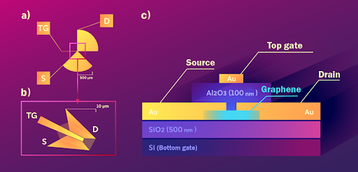
Study co-author Yakov Matyushkin from the MIPT Laboratory of Nanocarbon Materials сommented: “The detector consists of a silicon wafer 4 by 4 millimeters across, and a tiny piece of graphene 2 by 5 thousandths of a millimeter in size. The graphene is connected to two flat contact pads made of gold, whose bow tie shape makes the detector sensitive to the polarization and phase of incident radiation. Besides that, the graphene layer also meets another gold contact at the top, with a nonconductive layer of aluminum oxide interlaid between them.”
In microelectronics, this structure is known as a field transistor (fig. 1), with the two side contacts usually referred to as a source and a drain. The top contact is called a gate.

Figure 1. Inset (a) shows a top view of the device, with the sensitive region magnified in (b). The labels S, D, and TG denote the source, drain, and top gate. A side section of the detector is shown in (c). There are 1,000 nanometers (nm) in a micrometer (μm). Image Credit: Daria Sokol/MIPT Press Office
Terahertz radiation is a narrow band of the electromagnetic spectrum between microwaves and the far infrared light. From the applications standpoint, an important feature of T-waves is that they pass through living tissue and undergo partial absorption but cause no ionization and therefore do not harm the body. This sets THz radiation apart from X-rays, for example.
Accordingly, the applications traditionally considered for T-rays are medical diagnostics and security screening. THz detectors are also used in astronomy. Another emerging application is data transmission at THz frequencies. This means the new detector could be useful in establishing the 5G and 6G next-generation communication standards.
“Terahertz radiation is directed at an experimental sample, orthogonally to its surface. This generates photovoltage in the sample, which can be picked up by external measurement devices via the detector’s gold contacts,” commented study co-author Georgy Fedorov, deputy head of the MIPT Laboratory of Nanocarbon Materials. “What’s crucial here is what the nature of the detected signal is. It can actually be different, and it varies depending on a host of external and internal parameters: sample geometry, frequency, radiation polarization and power, temperature, etc.”
Notably, the new detector relies on the kind of graphene already produced industrially. Graphene comes in two types: The material can either be mechanically exfoliated or synthesized by chemical vapor deposition. The former type has a higher quality, fewer defects and impurities, and holds the record for charge carrier mobility, which is a crucial property for semiconductors. However, it is CVD graphene that the industry can scalably manufacture already today, making it the material of choice for devices with an ambition for mass production.
Another co-author of the study, Maxim Rybin from MIPT and Prokhorov General Physics Institute of the Russian Academy of Sciences is the CEO of graphene manufacturer Rusgraphene, and he had this to say about the technology: “The fact that it was CVD graphene that we observed plasma wave interference in, means such graphene-based THz detectors are fit for industrial production. As far as we know, this is the first observation of plasma wave interference in CVD graphene so far, so our research has expanded the material’s potential industrial applications.”
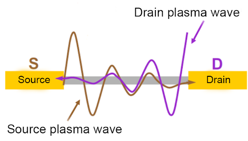
The team showed that the nature of the new detector’s photoresponse has to do with plasma wave interference in the transistor channel. Wave propagation begins at the two opposite ends of the channel (fig. 2), and the special geometry of the antenna makes the device sensitive to the polarization and phase of the detected radiation. These features mean the detector could prove useful in building communication and information transmission systems that operate at THz and sub-THz frequencies.

Figure 2. A schematic representation of plasma wave propagation in the transistor channel. Image Credit: Yakov Matyushkin et al./ACS Nano Letters
The study reported in this story was co-authored by researchers from the MIPT Laboratory of Nanocarbon Materials and their colleagues from Moscow State Pedagogical University, Ioffe Institute of the Russian Academy of Sciences, and the University of Regensburg, Germany. This research was supported by the Russian Foundation for Basic Research and the Russian Ministry of Science and Higher Education.