Feb 2 2021
NUS scientists have demonstrated a general approach for characterising the atomic structure, and electronic and magnetic properties of two-dimensional (2D) magnetic insulators using scanning tunnelling microscopy.
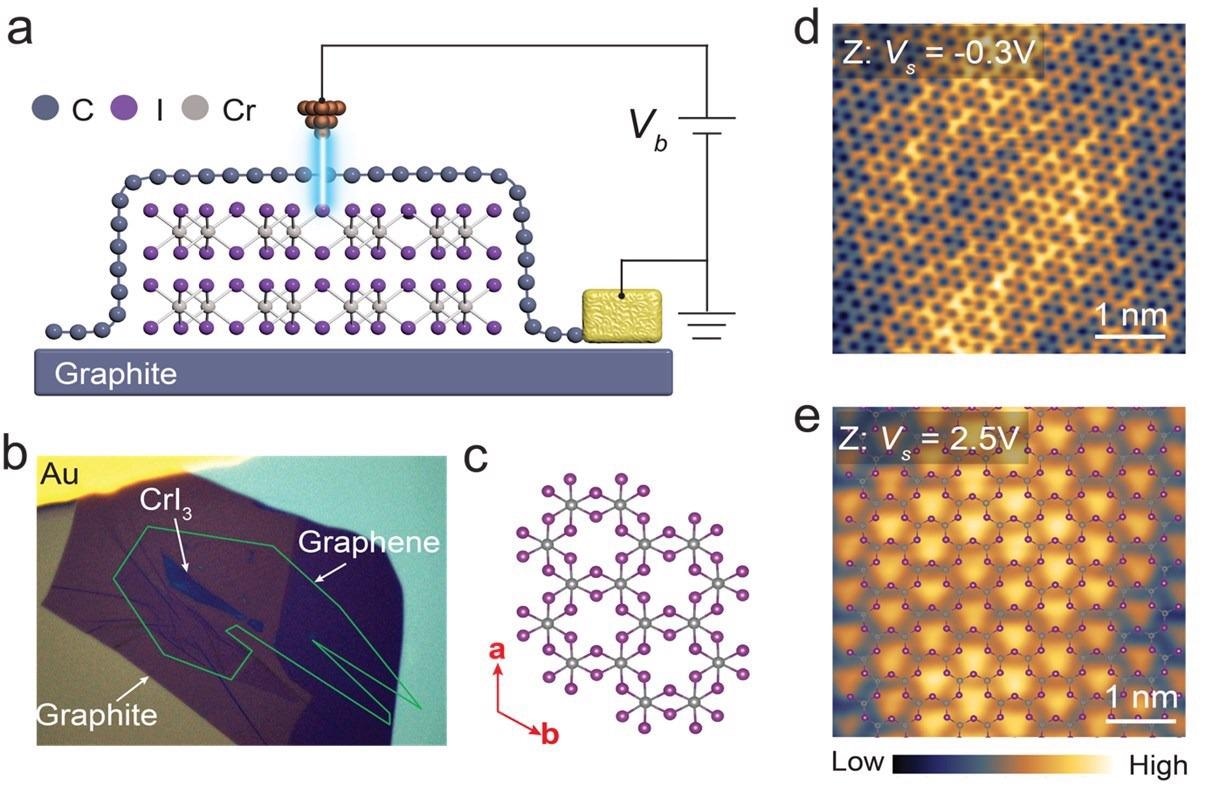
 Figure shows the van der Waals (vdW) heterostructure of G/FL-CrI3/Gr (G: graphene, FL: few layers, CrI3: chromium(III) iodide, Gr: graphite) used in the scanning tunnelling microscopy (STM) study. (a) The schematic illustration and (b) the optical image of the experimental setup. The sample consists of monolayer graphene covering the FL-CrI3 stacking on graphite flake (G/FL-CrI3/Gr). (c) The atomic structure of monolayer CrI3 (top view). Bias-dependent STM images of G/FL-CrI3/Gr shows the (d) graphene lattice – taken at Vs=-0.3V and (e) CrI3 lattice – taken at Vs=2.5V with superimposed atomic structure of monolayer CrI3 (I atoms on the bottom atomic plane are removed for clarity). [Credit: Nature Communications]
The recent discovery of 2D magnets and the development of van der Waals (vdW) heterostructure engineering offer unprecedented opportunities not only to explore the exciting physics of magnetism in reduced dimensions, but also to develop new-generation spintronic devices for quantum technology applications. Further developments in this area involve the atomic-level understanding of electronic and magnetic properties of 2D magnets and their heterostructures. Unfortunately, the direct application of conventional scanning tunnelling microscopy (STM) techniques to learn more about the material properties does not work well for 2D magnetic insulators. STM imaging relies on the quantum tunnelling effect, whereby electrons tunnel from the atomically-sharp tip to the conducting samples or vice versa. It cannot be applied to study insulating bulk materials as there is an absence of a conducting path.
A NUS research team led by Prof Jiong LU from the Department of Chemistry, NUS has demonstrated the application of STM to study insulating antiferromagnetic Chromium(III) iodide (CrI3) crystals by incorporating them with graphene-based vdW heterostructures (see Figure). This work is in collaboration with Prof Kostya S. NOVOSELOV from the Department of Materials Science and Engineering, NUS. Their technique expands on the capability of STM by enabling it for studying insulating materials to gain insights about the magnetic ordering in 2D magnets.
By capping the material under study with a single layer of graphene, the research team is able to obtain the stacking order and interlayer magnetic coupling of exfoliated CrI3 which is a few layers thick by using STM imaging at low temperature conditions. They also identified the magnetic structure and demonstrated that STM imaging can distinguish between the ferromagnetic and antiferromagnetic structures of CrI3 (few layers thick). This is due to the peculiar interaction of the magnetic states with the overlaying graphene.
Prof Lu said, “Our approach is general in nature, and it represents a breakthrough in the field of atomic-scale characterisation of the atomic structure, electronic and magnetic properties of various magnetic insulators and their vdW heterostructures. It can facilitate the development of 2D magnetic insulators for next-generation spintronic devices.”
Reference
Qiu Z; Holwill M; Olsen T; Lyu P; Li J; Fang H; Yang H; Kashchenko M; Novoselov KS*; Lu J*, “Visualizing atomic structure and magnetism of 2D magnetic insulators via tunneling through graphene” NATURE COMMUNICATIONS, 12(1), 1-7. Published: 2021.