A recent study published in the journal Materials Research Bulletin details that plasma etching results in a substantial increase in efficiency and performance of perovskite cells.

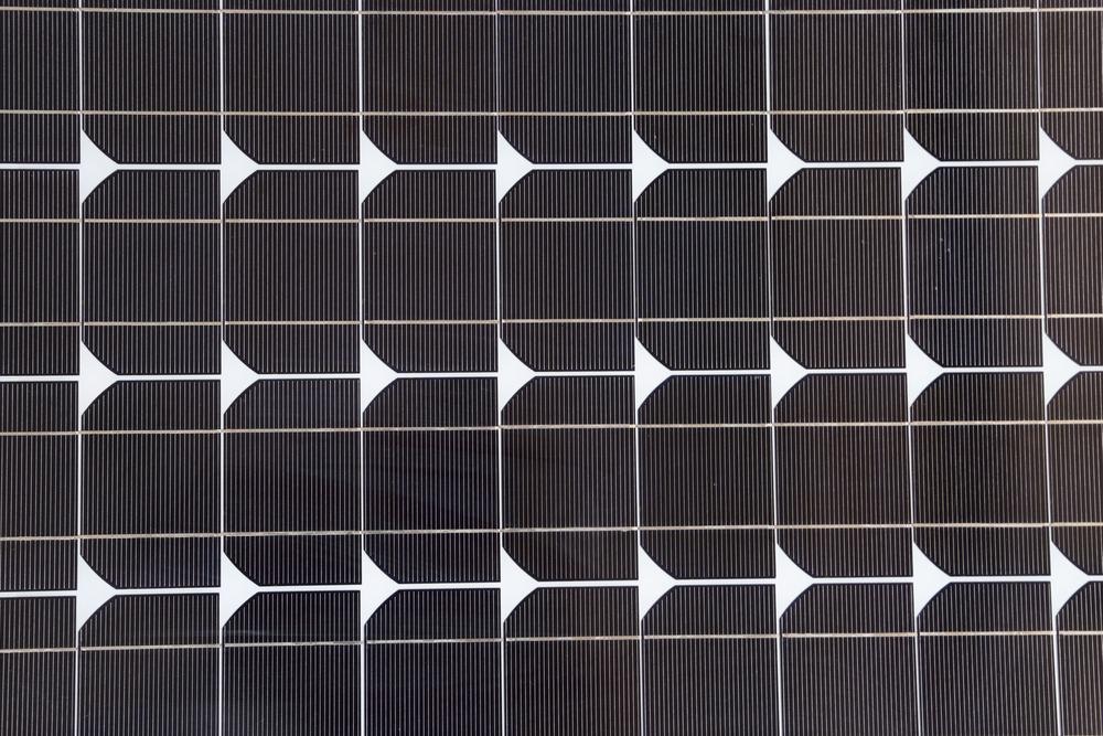
Study: Nanostructured Layer for High-performance Perovskite Solar Cells by Ar Plasma Etching. Image Credit: NJH Photography/Shutterstock.com
Organic-inorganic lead halide perovskite materials have attracted attention because of their excellent electronic and optical properties. This includes a wide-range absorption, controllable structural properties, long charge permeability duration, a high light absorption coefficient, and reduced exciton binding energy.
Limitations of Previous Technology
Although perovskite cells are utilized for various purposes, certain limitations restrict their usage. For instance, intense coupling would form on the surface between the perovskite absorbent film and the efficient charge distribution layer due to inadequate transport.
To overcome this problem, a framework layer with a thickness of 50-300 nm was used to extend the transport properties, which can assist to reduce carrier mobility length mismatches and improve photo-generated transport injection capability.
Research Findings
By sandwiching the produced semi-devices between two DC conductors, all of the plasma annealed nanostructured halide perovskites were obtained.
A popular approach for cleaning contaminants from the surfaces of substrates was to produce Ar plasma using electrostatic discharge.
It was discovered that as the treatment period increased, the interfaces of halide perovskites became coarser and surface nanocrystals became visible. Further ablation, however, demonstrated that the planar nanostructures flattened.
It is thought that the etching process began at the grain boundary and progressed as time passed. In particular, the elevated energy process of Ar plasma may readily break down perovskite substances and form nanostructures.
The results also implied that the high-energy Ar ions blasting did not produce surface defects.
Photovoltaic Assessment
The APE procedure was predicted to have a considerable influence on gadget photovoltaic efficiency.
The gadget with APE for 120 s was tested and contrasted to the control system with 0 s pretreatment due to its better visual and electrical features.
The device with APE for 120 s improved power conversion efficiency by 18.7 percent over the device for 0 s.
Optical Performance Assessment
The optoelectronic efficiency of the perovskite material was shown to be strongly connected to the photocatalytic efficiency of ultimate products.
While the absorption of samples was nearly identical, it was inferred that the suitable APE will not degrade the visual adsorption capability of the perovskite layer.
For the nanostructured perovskite layer, steady flow photoluminescence (PL) and time rectified photoluminescence (TRPL) were also investigated. The PL wilting of the PCBM/120 s Ar plasma treated perovskite material/electrode was greater than that of its equivalents.
The decay period of the pure perovskite material with 0 s APE was 48 ns, while the decay rate of the shorter PL lifetime of the 120 s scraped film was 23 ns.
The lowered PL intensity and PL lifespan revealed that the APE-created nanostructured layer had effectively expedited charge transport segregation. The larger contact area was responsible for the higher carrier separation efficiency. Researchers noted that more transportation centers may be available if the contact area is expanded.
It was demonstrated that Ar plasma ablation and the resulting nanoparticles on the surface of the cell layer did not affect its long-term durability. Furthermore, the structure and crystalline nature were unaffected by the etching procedure.
Limitations of Ar Plasma Etching
The downside of plasma etching, aside from the increased treatment cost when compared to wet-chemical surface modification, is poor specificity. Furthermore, extra droplets at the contact from the arc emitter are often created.
When utilizing plasma etching is not possible to adjust the ion concentration and free radical concentration separately in a capacitively connected plasma vessel as these two variables are linked. Instead, the plasma emission intensity is the sole parameter that may be changed.
Conclusions
In short, highly-efficient mesoporous perovskite solar cells utilizing the APE approach to build nanostructures on the surface of the perovskite layer without affecting its content or crystalline nature were successfully fabricated.
In the future, the APE approach suggested in this study could be used for various types of solar cells or optoelectronics.
Continue reading: Modeling Wing Nanostructures to Improve Solar Technologies.
Reference
Li, S. et al., (2021) Construction of Nanostructured CH3NH3PbI3 Layer for High-performance Perovskite Solar Cells by Ar Plasma Etching. Materials Research Bulletin, Volume 147. Available at: https://www.sciencedirect.com/science/article/pii/S0025540821004633
Disclaimer: The views expressed here are those of the author expressed in their private capacity and do not necessarily represent the views of AZoM.com Limited T/A AZoNetwork the owner and operator of this website. This disclaimer forms part of the Terms and conditions of use of this website.