Chip-like oversized probes in atomic force microscopy (AFM) perturb the tuning fork's oscillations, resulting in poor sensing. Hence, restoring the oscillatory characteristics in the oversized chip-like probes is critical to regaining high sensitivity. In an article recently published in the journal Microsystems & Nanoengineering, the authors demonstrated a new approach to using a "tip-on-chip" probe by employing three steps: tuning-fork rebalancing, refurbished holder-sensor fixation, and electrode reconfiguration.

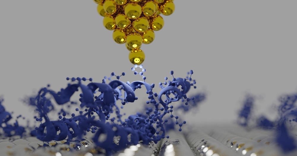
Study: Enhancing sensitivity in atomic force microscopy for planar tip-on-chip probes. Image Credit: sanjaya viraj bandara/Shutterstock.com
Functionalization of Probes for Sensitivity
Scanning probe microscope (SPM) has undergone many modifications, such as silicon (Si)-coated and magnetically coated tips, based on their applications to enhance the sensitivity in AFM.
Other advanced forms with tip metallization include superconductive scanning tunneling microscopy (STM), Kelvin probe force microscopy (KPFM), and conductive atomic force microscopy (CAFM). Tip conversion from passive to active element with current control is the most recent development in probe metallization.
Despite the unique solutions provided by the functionalized probes, the fragility of soft Si-cantilever or the tiny needle-like tip limits their applicability. Thus, the solution to this drawback is micro-tailoring structures like scanning thermal microscope (SThM) for quantitative sensing and advanced tip functionalization.
Probes in planar forms are alternatives to conventional SPM tips. The wafer-shaped planar probe has a sharp cornered scanning tip having high resolution. Additionally, the planar probe can combine nanotailoring and ultra-thin film technology at its sharp tip.
Novel "Tip-on-chip" Approach
In the present paper, the authors demonstrated an upgraded fabrication method to enable a system with high sensitivity and broad compatibility. This method provides atomic resolution in AFM and STM at room temperature. The new approach consists of three steps: tuning-fork rebalancing, revamping holder-sensor fixation, and electrode reconfiguration.
The authors recovered the tuning fork frequency and regained high Q-factor values in air and ultra-high vacuum conditions by mass rebalancing.
Research Findings
In the present study, the authors demonstrated the capabilities of a novel approach for its broad compatibility and high sensitivity. They performed several scans in AFM and STM modes for a range of samples from crystals to polymers, using air and ultra-high vacuum (UHV) setups for the structural measurements.
The new approach proved to be versatile and facile to adapt to two different setups, providing an insight into the compatibility of the novel approach.
The results revealed that atomic resolution was achieved by using planar probes in STM and AFM mode. The high resolution achieved reveals that the oversized chip-like probe with a cleaved tip is of nanoscale radius. Similarly, the Si calibration sample raster scans profile the planar probe tip convolution with a large opening angle.
The tuning fork's robustness emanates such a high versatility and stability, thus preventing the jump-to-contact behavior of the tip. The control unit performed on reliable surfaces for consecutive measurements in constant frequency and height mode.
The new approach to utilizing a highly sensitive tuning fork in AFM can facilitate the application of oversized active chip-like probes. Furthermore, the probe attached area reveals the flexibility in employing a wide range of tip-on-chip designs, from coherent current-carrying wire to fabricating the tip with an electronic circuit.
The planar probes facilitate the applicability of ultra-thin film engineering, which otherwise is not allowed in the pyramidal or conical geometry of conventional AFM tips. The high precision of layer growth provides a wide selection of materials in multi-layer stacks and unmatched adjustability. In addition to passive sensitivity, the planar probes' film engineering allows tailoring of the micro-circuit. Previous studies revealed that the tip structured with a circuit generates a thermal gradient suitable for thermomechanical patterning.
Moreover, the microwire through which the current flows function as a heat-sensing element. The current flow through the microwire allows it to serve as a magnetic element at the tip. Such localized fields can control the spin texture of thin films that are ferromagnetic. The thin ferromagnetic coating-induced magnetic field is at the probe's tip.
Conclusion
To conclude, the new approach of combining a restored tuning-fork sensor and floating-like holder-fixation provided improved AFM performance. The retuned method provided greater sensitivity and compatibility for a different system. Moreover, the reconfigured electrodes reduced energy access and energy dissipation for the tip-on-chip probe.
Signal separation and oscillation feedback for tip-on-chip control was due to electrically disconnected lower and upper prongs electrodes.
Significantly improved Q-factor values enhanced AFM sensitivity, which did not match the previous configuration with chip-like probes. The incorporation of tip-on-chip with a robust tuning fork widens the sustainability and compatibility.
Reference
Çiftçi, H. T., Verhage, M., Cromwijk, T., Van, L. P., Koopmans, B., Flipse, K., and Kurnosikov, O. (2022) Enhancing sensitivity in atomic force microscopy for planar tip-on-chip probes. Microsystems and Nanoengineering 8, 51.https://www.nature.com/articles/s41378-022-00379-x
Disclaimer: The views expressed here are those of the author expressed in their private capacity and do not necessarily represent the views of AZoM.com Limited T/A AZoNetwork the owner and operator of this website. This disclaimer forms part of the Terms and conditions of use of this website.