The etching process removes the overlying sacrificial metal and exposes the transfer-free graphene required for industrial applications. In an article recently published in Chemistry of Materials, researchers used a microfluidic system to design a laminar flow-assisted etching method to remove the metal layer deposited on graphene.

Study: Laminar Flow-Assisted Metal Etching for the Preparation of High-Quality Transfer-Free Graphene. Image Credit: Evgeniy Zebolov/Shutterstock.com
Properties of Graphene
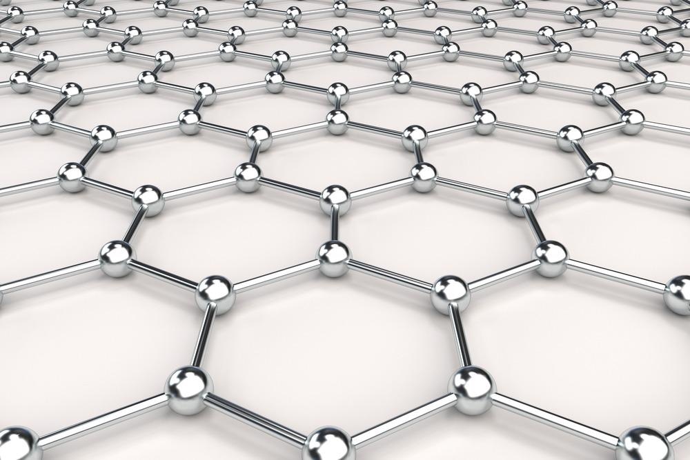
Graphene is a carbon allotrope with a honeycomb lattice structure. Its unique physicochemical properties are useful for a wide range of applications in optics, electronics, energy storage, and molecular barriers. Industrially scalable high-quality graphene is prepared via chemical vapor deposition (CVD), using catalytic metal substrates. Since most graphene applications involve semiconductors and insulators, an additional process is required to transfer the synthesized graphene to target substrates from the catalytic method.
Owing to the straightforward process and affordability, polymer-supported methods are widely used to transfer graphene. However, this method has major drawbacks, such as the retention of polymer residues on the surface of graphene and the structural defects induced by imperfect transfer, which deteriorate the quality of the transferred graphene.
Laminar Flow-Assisted Metal Etching
In the present study, the researchers exploited the laminar flow in a microfluidic system. They developed an etching method to produce continuous and patterned transfer-free graphene, with conformal morphology, on a metal substrate with minimal structural defects. Furthermore, the team demonstrated that apart from achieving high-quality graphene, this laminar flow-assisted etching process was highly compatible with automatic operation, high reproducibility, reduced reagents, and highly scalable.
Research Findings
To remove the catalytic metal films and expose transfer-free graphene whose growth was at the interface of metal- silica/silicon (SiO2/Si) interface, the researchers developed an etching process conducted in a microfluidic system. The transfer-free graphene with a metal cover was grown on a Si substrate, that was placed in an etching chamber for subsequent metal removal. Moreover, the etching chamber’s fluid field was dominated by the laminar flow, which allowed the etching of the metal film in a smooth and controlled manner, avoiding any defects in graphene.
Additionally, the microfluidic system allows a multistep etching process by switching the injected solution between rinse buffers and etchants. This multistep etching process enables transfer-free graphene growth kinetics. The presence of graphene on the copper film’s surface was confirmed by the Raman spectra G and 2D bands observed at approximately 1578 and 2695-centimeter inverse, respectively.
The first etching was conducted for 5 minutes, using 0.1 molar ammonium persulfate (APS) as the etchant, injected at 0.05 milliliter per minute infusion rate. This sample did not exhibit Raman signals of graphene, but broad D ad G bands were found approximately at 1355 and 1578-centimeter inverse, respectively.
The copper (Cu) background signal was notable, indicating the removal of the outer Cu surface while retaining the bulk of the film. These observations also infer that the graphene on the outer surface is removed along with the outermost Cu layer. The detection of amorphous carbon in the bulk of Cu film indicated the active carbon species diffusion in Cu film, a critical step in transfer-free graphene growth kinetics. After the complete removal of Cu film, residual graphene films were not formed on the Cu surface.
The researchers conducted a finite element method (FEM) simulation to determine the characteristics of laminar flow-assisted etching. They calculated the fluid flow fields and reactant mass transport to determine the depletion of metal films. Additionally, time-dependent simulations were conducted on depleting metal films to determine the kinetic properties of the proposed etching process.
After etching the Cu, deionized (DI) water was injected with the infusion rate of 0.1 milliliters per minute to rinse off the transfer-free graphene that was exposed on the SiO2 substrate. Generally, persulfate anions show a peak below 250 nanometers; hence the water rinsing for approximately 30 minutes resulted in the disappearance of a peak at approximately 214 nanometers, indicating the removal of persulfate anions. X-ray photoelectron spectroscopy (XPS) was performed to ensure the effective removal of Cu film by the APS-based microfluidic etching process. The spectrum obtained from XPS revealed peaks of carbon (C) 1s at 284 electronvolts from graphene, oxygen (O) 1s at 532 electronvolts, Si 2s at 154 electronvolts, and Si 2p at 103 electronvolts from the SiO2 substrate.
Conclusion
To conclude, the researchers developed a convenient method to remove metal films that covered the transfer-free graphene, whose growth was at the interface of Cu−SiO2/Si, wherein the microfluidic etching system was employed. Owing to the incorporation of a laminar flow system, this method had a stationary surface with negligible flow velocity and the mass transport of etchants towards the metal surface was in a diffusion-controlled manner. This allowed the etching of Cu films from the intrinsic transfer-free graphene, which was smooth and well-controlled. Subsequently, the transfer-free graphene detachment from the underlying SiO2 was avoided effectively.
Reference
Fang-Chi Ding, Cheng-Yu Dai, Chun-Lung Yao, Cheuk Yui Lai, and Chiao-Chen Chen (2022). Laminar Flow-Assisted Metal Etching for the Preparation of High-Quality Transfer-Free Graphene. Chemistry of Materials. https://doi.org/10.1021/acs.chemmater.2c00450
Disclaimer: The views expressed here are those of the author expressed in their private capacity and do not necessarily represent the views of AZoM.com Limited T/A AZoNetwork the owner and operator of this website. This disclaimer forms part of the Terms and conditions of use of this website.